
The photovoltaic inverter is a very important device in the photovoltaic system. Its main function is to convert the DC power emitted by the photovoltaic modules into AC power. In addition, the inverter is also responsible for detecting the operating status of the components, power grid, and cables, and the communication with the outside, etc.
Inverter IGBT plays the role of power conversion and energy transmission in the inverter, and is the heart of the inverter. TYCORUN's all series of inverters, including 3000 watt solar inverter and 2000 watt inverter pure sine wave, are using high quality IGBT modules. If you want to know more about inverter IGBT, let's have a look today.
Main content:
1. What is inverter IGBT?
Inverter IGBT is the abbreviation of insulated gate bipolar transistor. It is a three-terminal semiconductor switching device that can be used for efficient and fast switching in a variety of electronic equipment.
IGBTs are primarily used in amplifiers for switching/processing complex waveforms via pulse width modulation (PWM). The most popular and common electronic components in practical applications are bipolar junction transistors (BJT) and MOS tubes, and inverter IGBT can be regarded as a fusion of BJT and MOS tubes. Inverter IGBT has the input characteristics of BJT and the output characteristics of MOS tubes.
2. Internal structure of inverter IGBT
An inverter IGBT has three terminals (collector, emitter and gate) with metal layers attached to them and the metal material on the gate terminal has a silicon dioxide layer. The structure of inverter IGBT is a four-layer semiconductor device. Four-layer devices are implemented by combining PNP and NPN transistors, which form a PNPN arrangement.
As shown in the figure above, the layer closest to the collector area is the (p+) substrate, which is the injection area. Above it is the N drift area, including the N layer. The injection area injects most of the carriers (hole current) from the (p+) into the N- layer. The thickness of the drift area determines the voltage blocking capability of the inverter IGBT.
Above the drift area is the body area, which consists of the (p) substrate, close to the emitter, and inside the body area, the (n+) layer. The connection point between the injection area and the N-drift area is J2. Similarly, the node between the N-area and the body area is node J1.
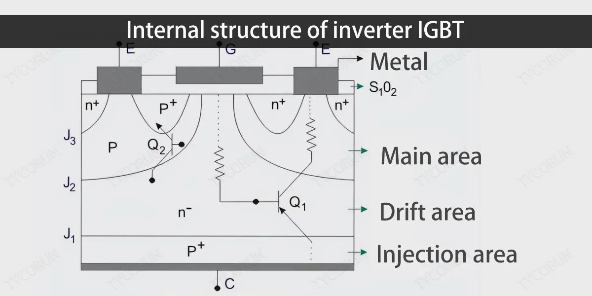
It is important to note that the structure of an inverter IGBT is topologically similar to a MOS gated thyristor. However, thyristor operation and function are suppressable, which means that only transistor operation is allowed over the entire device operating range of the inverter IGBT. IGBTs are preferable to thyristors because thyristors wait for fast switching at zero crossing.
3. How Inverter IGBT works
An inverter IGBT works by activating or deactivating its gate terminal to turn it on or off. If a positive input voltage passes through the gate, the emitter keeps the driver circuit on. On the other hand, if the gate terminal voltage of the inverter IGBT is zero or slightly negative, it will shut down the circuit application. Since an IGBT can be used as both a BJT and a MOS tube, the amount of amplification it achieves is the ratio between its output signal and the control input signal.
For a traditional BJT, the amount of gain is roughly the same as the ratio of output current to input current, while a MOS transistor has no input current because the gate terminal is isolated from the main channel carrying current. The figure below explains the working principle of inverter IGBT and the operating range of the entire inverter IGBT device.
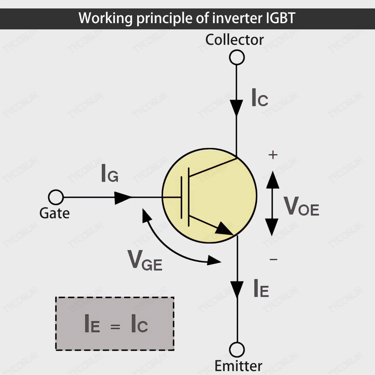
When the inverter IGBT works only when there is voltage supply on the gate terminal, it is the gate voltage (VG). As shown in the figure above, once the gate voltage (VG) is present, the gate current (IG) increases, which then increases the gate-emitter voltage (VGE). Therefore, the gate-emitter voltage increases the collector current (IC). Therefore, the collector current (IC) reduces the collector-to-emitter voltage (VCE).
It is important to note that IGBTs have a voltage drop similar to that of a diode, typically on the order of 2V, increasing only with the logarithm of the current. The inverter IGBT conducts the reverse current using a freewheeling diode, which is placed at the collector-emitter terminal of the IGBT.
4. Characteristics of IGBT
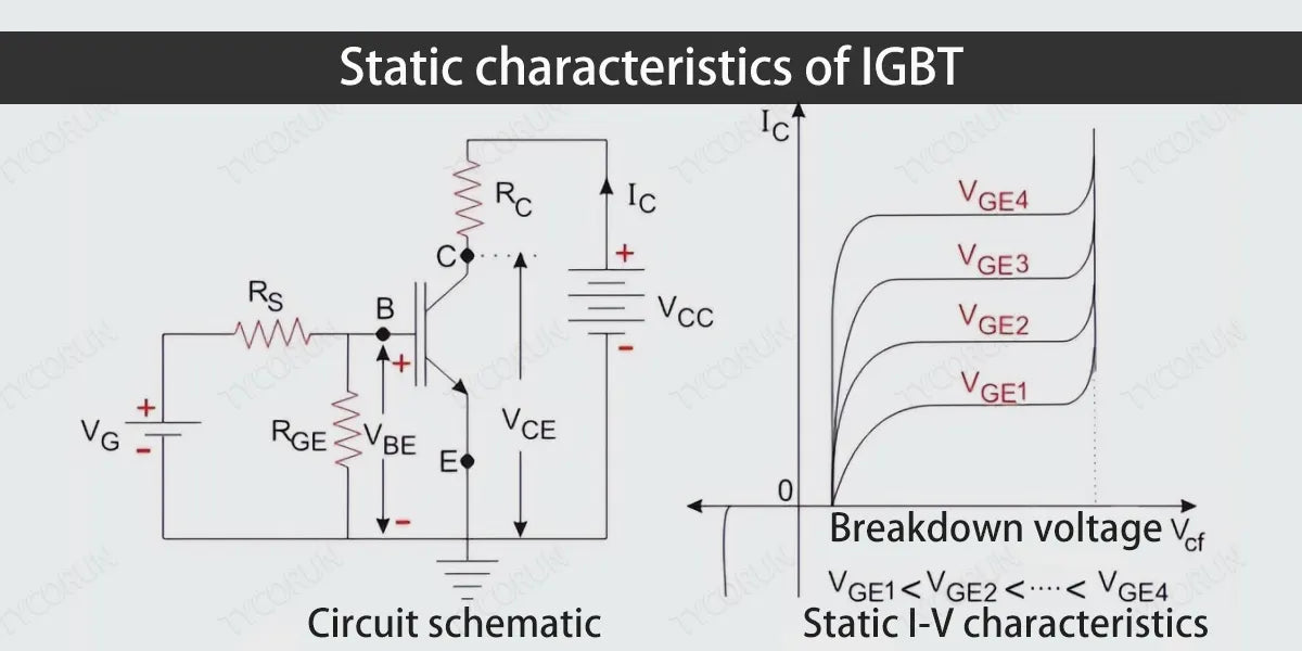
- Static VI characteristics
The figure below shows the static VI characteristics of an n-channel IGBT along with a circuit diagram labeled with parameters. The parameter that is kept constant in the figure is VGE because the inverter IGBT is a voltage controlled device. When the IGBT is in off mode (VCE is positive and VGE < VGET), the reverse voltage is blocked by J2 and when it is reverse biased, which means VCE is negative, J1 blocks the voltage.
- Switching characteristics
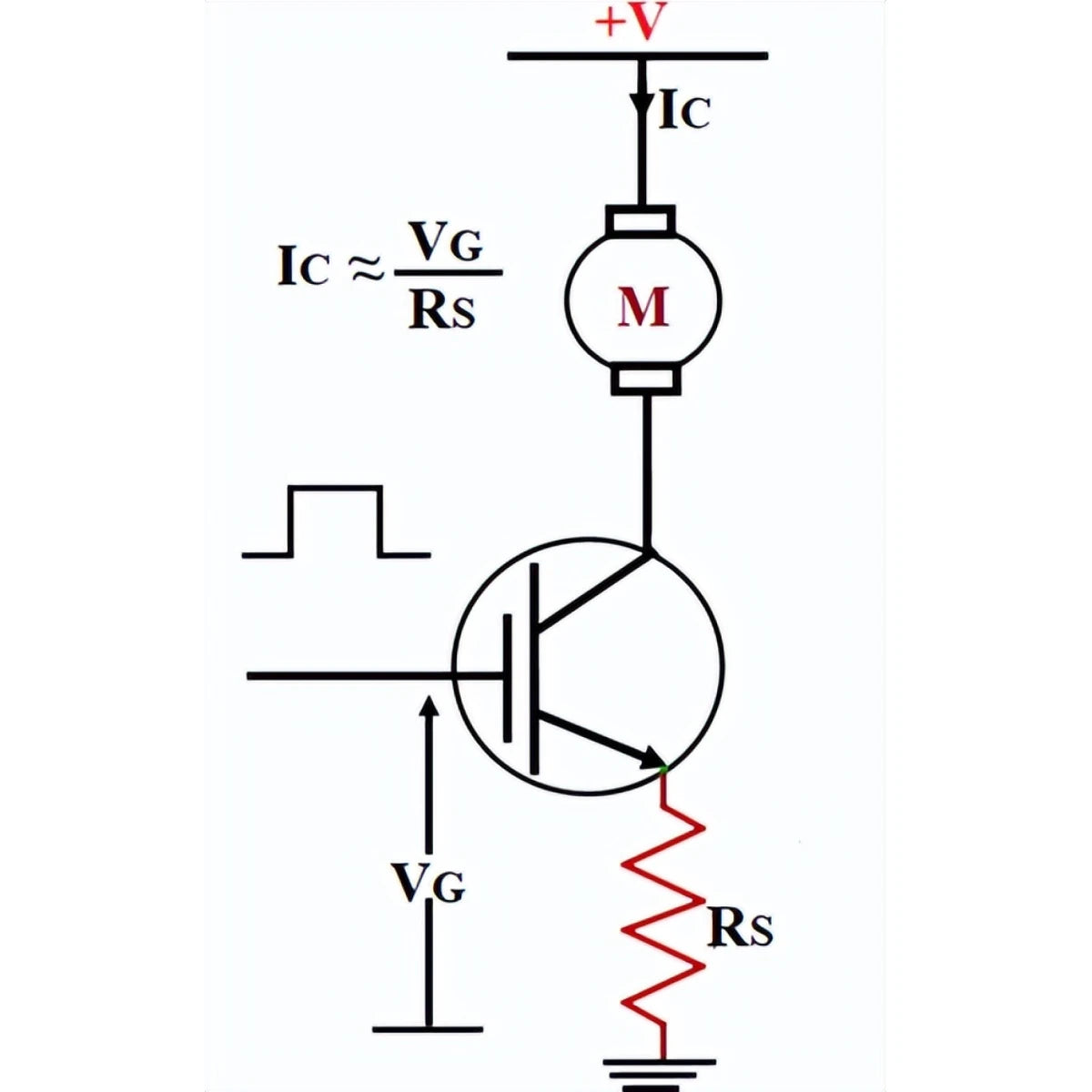
Inverter IGBT is a voltage controlled device, so it only requires a small voltage to the gate to remain on. Since it is a unidirectional device, IGBT can only switch current in the forward direction from collector to emitter. A typical switching circuit of an IGBT is shown below, the gate voltage VG is applied to the gate pin to switch the motor (M) from the supply voltage V+. Resistor Rs is used roughly to limit the current through the motor.
Typical switching circuit diagram of an inverter IGBT is as below:
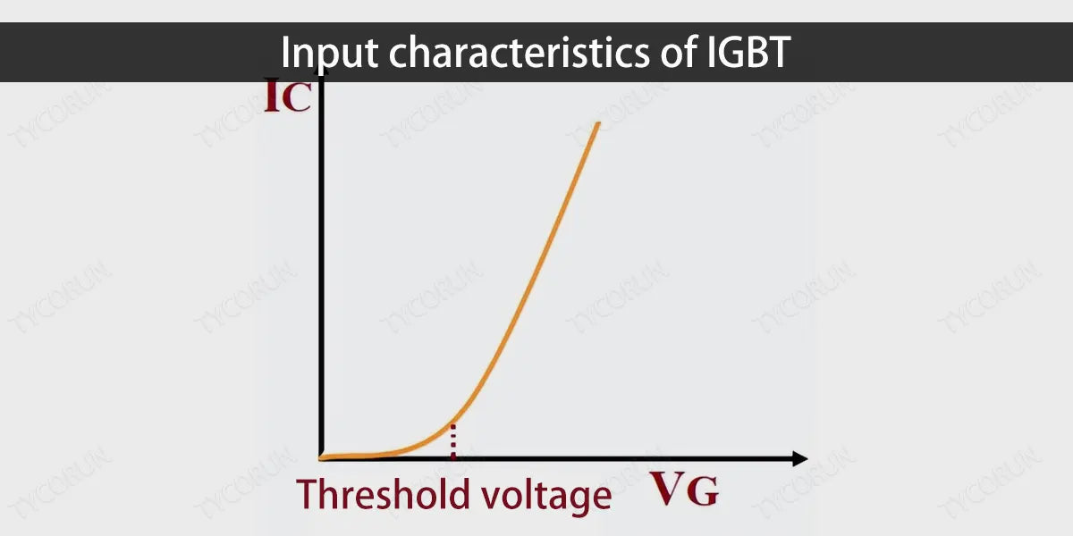
- Input characteristics
The following figure shows the input characteristics of an inverter IGBT. Initially, when no voltage is applied to the gate pin, the IGBT is in the off state and no current flows through the collector pin. When the voltage applied to the gate pin exceeds the threshold voltage, the inverter IGBT starts conducting and the collector current IG starts flowing between the collector and emitter terminals. The collector current increases relative to the gate voltage as shown in the figure below.
- Output characteristics
Since inverter IGBT operation is depend on voltage, only a very small amount of voltage needs to be applied to the gate terminal to remain conductive. IGBTs are in contrast to bipolar power transistors, which require a continuous base current flow in the base area to maintain saturation. An IGBT is a unidirectional device, meaning it can only switch in the "forward" direction (from collector to emitter).
IGBT is exactly the opposite of MOS tube with bidirectional current switching process. The forward direction of the MOS tube is controllable, but the reverse voltage is uncontrollable. Under dynamic conditions, when the inverter IGBT is turned off, it may experience latch-up current, which is when the continuous on-state drive current appears to exceed a critical value.
In addition, when the gate-emitter voltage is lower than the threshold voltage, a small amount of leakage current flows through the IGBT. At this time, the collector-emitter voltage is almost equal to the supply voltage. Therefore, the four-layer device IGBT operates in the cut-off area.
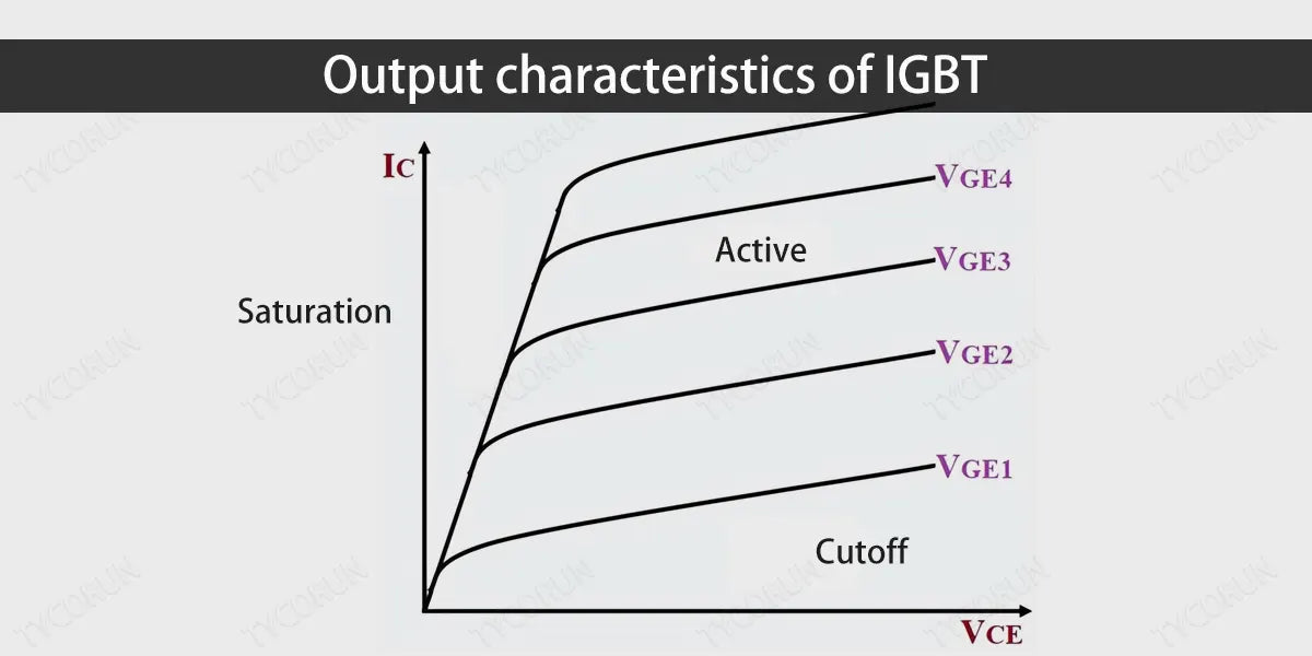
The output characteristics of IGBT are divided into three stages:
Stage 1: When the gate voltage VGE is zero, the IGBT is in the off state, which is called the cut-off area.
Stage 2: When VGE increases, if it is less than the threshold voltage, there will be a small leakage current flowing through the IGBT, but the IGBT is still in the cut-off area.
Stage 3: When VGE increases beyond the threshold voltage, the IGBT enters the active area and current begins to flow through the IGBT. As shown in the figure above, the current will increase as the voltage VGE increases.
5. Pros and cons of inverter IGBT
IGBT has the advantages of BJT and MOS tube.
Pros:
- Better capabilities of handling voltage and current;
- Very high input impedance;
- High currents can be switched using very low voltages;
- Has no input current and low input losses;
- The gate drive circuit is simple and cheap, reducing gate drive requirements;
- Easily turned on by applying a positive voltage, and easily turned off by applying a zero or negative voltage;
- Very low on-resistance;
- High current density, enabling smaller chip sizes;
- Higher power gain than BJT and MOS tubes;
- Higher switching speed than BJT;
- High current levels can be switched using low control voltages;
- Enhanced conductivity due to bipolar nature;
- Safer.
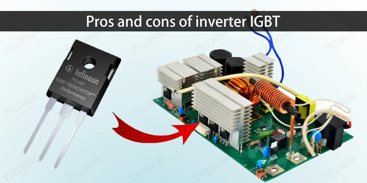
Cons:
- The switching speed is lower than that of MOS tubes;
- Unidirectional, cannot handle AC waveforms without additional circuitry;
- Cannot block higher reverse voltages;
- More expensive than BJT and MOS tubes;
- Similar to the PNPN structure of the thyristor, it has a latch problem;
- The turn-off time is longer than PMOS tubes.
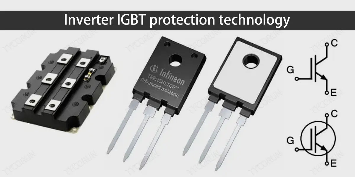
6. Inverter IGBT protection technology
Inverter IGBT is very sensitive to the temperature and current of the device, and if it exceeds the standard, it may not be repairable. Therefore, IGBT is the key protection object of the inverters that work with lawn mower battery or golf cart battery, or other power wheels battery. The core application of IGBT protection technology in photovoltaic inverters is reflected in four aspects: drive protection, overcurrent/short circuit protection, overtemperature protection, and mechanical fault protection, as detailed below.
- Driver protection
The IGBT itself is a current switching device, and the switching time is controlled by the inverter's CPU. However, the DSP output is a PWM signal, which is very fast but has insufficient power. The main function of the driver is to amplify the PWM signal.
The IGBT controls a large high-frequency and large current, which will generate electromagnetic interference signals. The driver is very close to the IGBT, so the driver circuit must have an isolation function. Current driver isolation solutions include optocouplers, optical fibers, pulse transformers, and magnetic couplings, etc.
- Over current/short circuit protection
When designing IGBTs, a margin of more than 10% is generally left for the current. However, when the inverter is working, due to component and load short circuits and load side faults, overcurrent occurs. There is a particularly large inductive load on the load side, and there is a large harmonic current during startup and shutdown.
At this time, a sharp rise in the inverter output current will cause the IGBT's operating current to rise sharply accordingly. Short circuit of inverter IGBT is divided into two situations:
① A direct connection occurs in the bridge arm of the converter, which is called a type I short circuit;
② The short-circuit point of the converter occurs on the load side, and the equivalent short-circuit impedance is large, which is called a Class II short circuit. Class II short circuit can generally also be considered as a serious overcurrent in the inverter.
When a short circuit occurs, if no relevant measures are taken, the inverter IGBT will quickly enter desaturation, and the transient power consumption will exceed the limit and be damaged, because the IGBT can withstand overcurrent for only a few microseconds.
Therefore, when a short circuit occurs, the IGBT must be turned off as soon as possible, and the turn-off speed must be gentle to ensure that the current change rate is within a certain range, so as to avoid turning off too fast and causing the voltage stress to exceed the limit and damage the IGBT.
- Over-temperature protection
When the ambient temperature of the inverter is too high, the heat dissipation of the inverter will be poor, and continued overheating will cause damage to the IGBT. If the device continues to be short-circuited, the power consumption generated by the large current will cause a temperature rise.
If the chip temperature exceeds the intrinsic temperature of silicon (about 250°C), the device will lose its blocking ability and the gate control will not be able to protect it, resulting in IGBT failure. There are two main aspects to consider when designing for over-temperature protection:
① Strengthen and improve the heat dissipation conditions of IGBT tubes, including air duct design, design and production of radiators, and strengthening the refrigeration, etc.
② Design an overheat detection protection circuit and use the thermistor built into the IGBT module to measure the IGBT heat dissipation temperature. This method is very accurate. When the temperature exceeds the set value, the IGBT will be turned off to stop working.
- Mechanical failure protection
In order to facilitate the heat dissipation, IGBTs are connected through screws and installed on the radiator. The connection strength of this screw must be just right, neither too strong nor too light. If the force is too strong, the IGBT will be damaged; if the force is too light, vibration may cause poor contact, increase thermal resistance, and overheat the device during transportation and installation.
When installing IGBT, a special screwdriver is used. According to the IGBT model, the corresponding torque is used to ensure that the IGBT connection is firm and will not be damaged. Inverter IGBT is the most easily damaged device in the inverter, and it is also the most expensive and most critical device in the inverter. Therefore, in order to better protect the IGBT, the inverter must take more corresponding protection measures.
All our inverters deliver stable and safe power output. You can check our products according to your need: inverter 3000w, 2000w inverter, 1000w inverter, 500w car inverter
Related posts: 12 volt 100ah lithium battery, 24 volt marine battery, home solar power system