

When power supply engineers choose to use power MOSFETs, which is widely used in 2000w inverter or 3000w inverter that work with LFP battery, to design power supplies, most of them make preliminary decisions directly based on the three parameters of power MOSFETs: maximum withstand voltage, maximum conduction current capability, and conduction resistance. But in fact, the switching loss test of MOSFET/IGBT is a very critical point in power supply debugging of home solar power system and device evaluation.
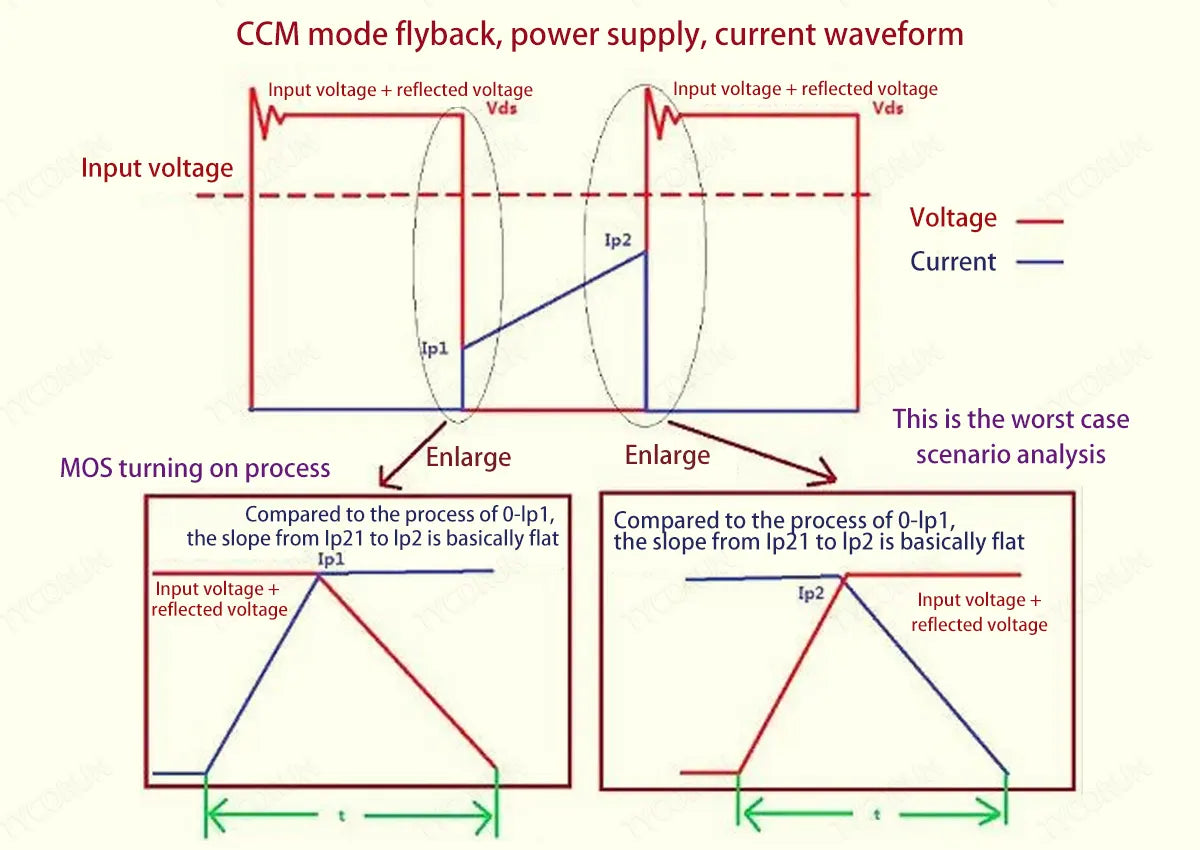
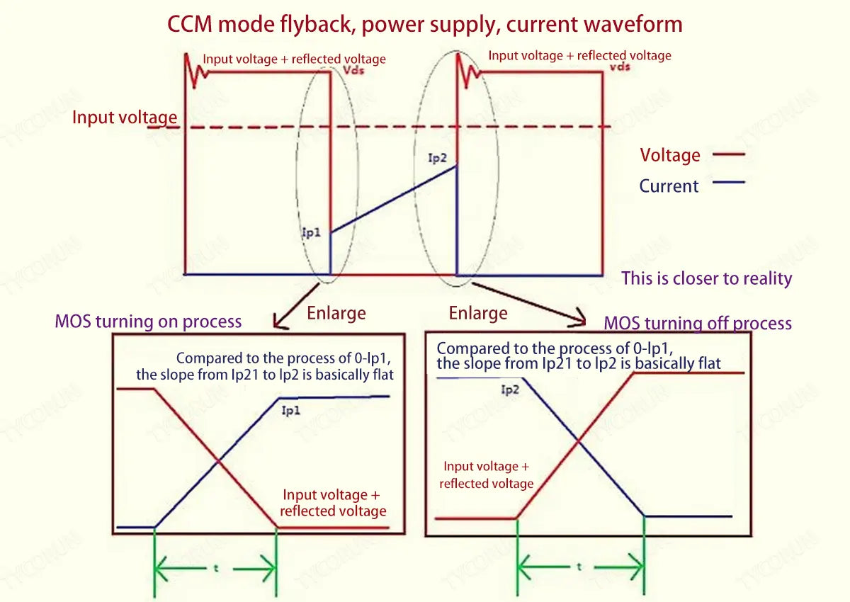
However, many engineers rely on the perceptual perception of manual calculation when measuring switching loss. The most common MOSFET switching loss are turn-on loss and turn-off loss. Today, we will use the turn-on loss and turn-off loss of flyback CCM mode. Let’s deduce the formula based on the cutting loss, I hope it can give you some reference.
Main content:
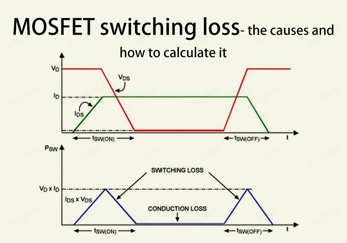
1. Causes of MOSFET switching loss
Turn-on loss refers to that when a non-ideal switch tube is turned on, the voltage of the switch tube does not drop to zero immediately, but has a falling time. At the same time, its current does not rise to the load current immediately, and there is a rise time.
During this period, the current and voltage of the switch tube have an overlap area, which will cause loss. This loss is the turn-on loss. By analogy, we can get the reasons for the turn-off loss. Another meaning of switching loss is that in switching power supplies, when switching large MOSFET diode, parasitic capacitance needs to be charged and discharged, which will also cause losses.
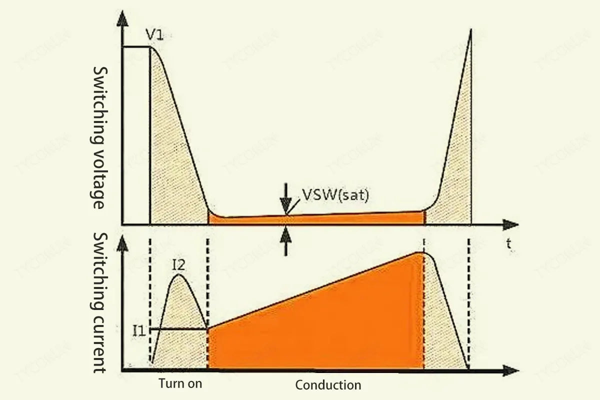
Analysis of the worst case
The figure below shows the overlapping process of current and voltage during switching. What this figure describes is actually the worst case. When it is turned on, the voltage of the MOS tube does not start to drop until the current of the MOS tube rises to I1. When it is turned off, the voltage of the MOS tube starts to drop. After the voltage rises to Vds, the MOS tube current begins to decrease.
① MOS tube turning on process:
Stage 1: The voltage remains unchanged and the current rises (the voltage remains unchanged at Vds, and the current rises from 0 to Ip1). When the MOS is turned on, the current quickly rises from zero to Ip1. During this process, the DS voltage of the MOS does not change to Vds.
Stage 2: The current remains unchanged and the voltage drops (the current remains unchanged at Ip1, and the voltage drops from Vds to 0). After the current rises to Ip1, the rising slope of the current (Ip1-Ip2 segment) is very slow relative to the moment 0-Ip1. We can approximately think that the slope that continues to rise after rising to Ip1 is 0, and the current is basically considered to be unchanged at Ip1. At this time, the DS voltage of the MOS tube begins to rapidly drop to 0V.
② MOS tube turning off process:
Stage 1: The current remains unchanged and the voltage rises (the current remains unchanged at Ip2, and the voltage rises from 0 to Vds). The voltage quickly starts to rise from 0 to the highest voltage Vds. The same as when it is turned on, the current of the MOS during this process basically does not change to Ip2.
Stage 2: The voltage remains unchanged and the current decreases (the point voltage remains unchanged at Vds, and the current drops from Ip2 to 0). The voltage remains unchanged at Vds, and the current quickly drops from Ip2 to 0 with a large downward slope.
As for the turn-off and turn-on crossover time t, the estimation process will be given below. Please refer to the figure below:
- When turning on: the rising process of current 0-Ip1 and the falling process of voltage Vds-0 occur simultaneously.
- When turning off: the rising process of voltage 0-Vds and the falling process of current from Ip2-0 occur simultaneously.
2. Calculation of MOSFET switching loss at turn-on
Let’s first locate the turning on time t1. It seems that if we use the average method to calculate it, we can directly see that Ip1/2 × Vds/2 *t1*fs. In fact, this is not accurate. The calculation is that each instant within time t corresponds to a power, and then all the instantaneous powers during this period are accumulated and then divided by the switching period T or multiplied by the switching frequency fs.
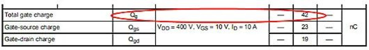
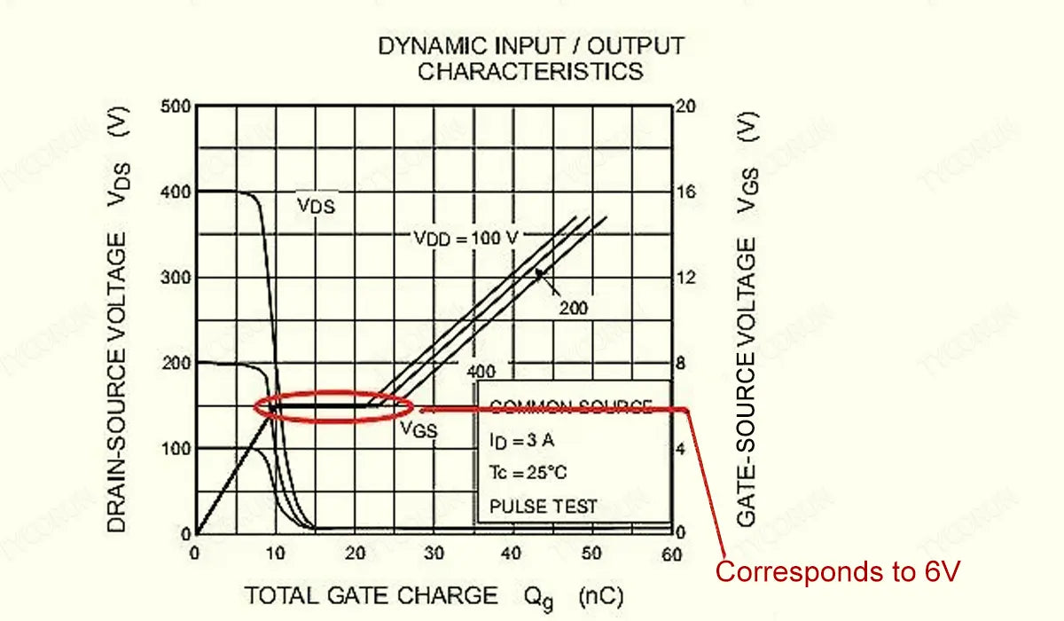
Next, let me talk about the estimation method of t1. The idea is to calculate time t1 based on the total gate charge given in the MOS tube datasheet, and use the formula Qg=i*t to calculate.
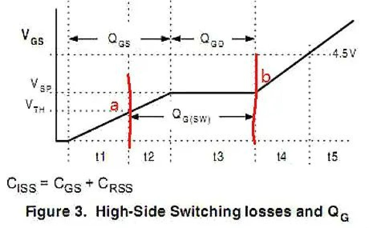
The picture above shows the driving process. Vth is the turn-on threshold of the MOS tube, and Vsp is the Miller platform of the MOS tube. In fact, the process from the beginning of conduction to saturated conduction of the MOS tube is from the driving voltage point a to point b. The total gate charge Gg can be found in the datasheet of the MOS tube.
The driving current is determined based on your actual driving circuit.
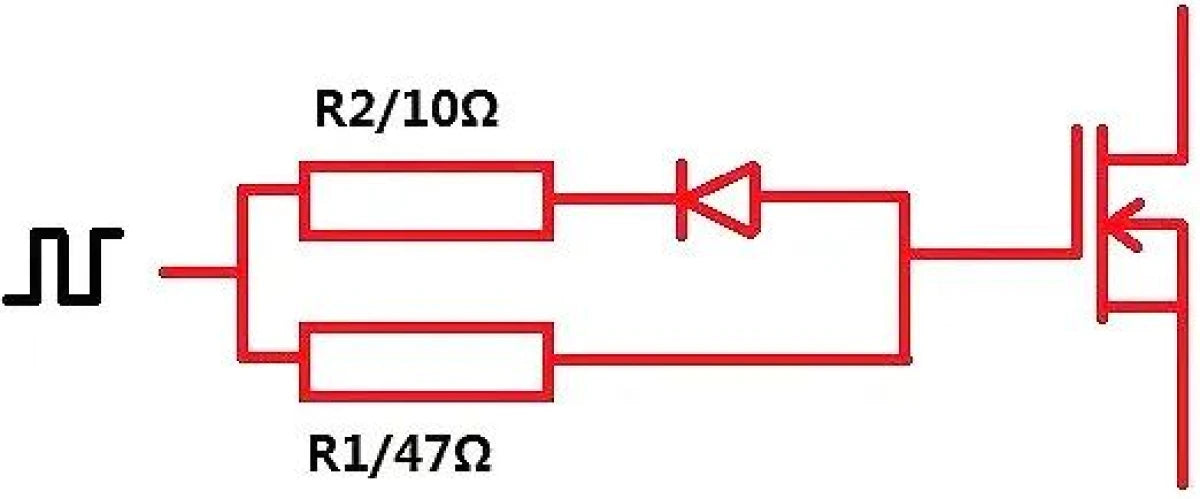
The current i can be calculated based on the value of your drive resistor R1 and the Miller plateau voltage. The Miller platform voltage Vsp can also be found in the datasheet of the MOS tube.
Then according to the actual driving voltage (actually it is approximately equal to the chip Vcc supply voltage), before the actual voltage is made, you can preset one yourself in the theoretical estimation stage, such as the preset 15V. When calculating, the section from Vth to Vsp is approximately regarded as equal to Vsp, and then it is simple to calculate i.
i=(Vcc-Vsp)/R1
At this moment, the driving current i has been calculated, and then the plateau time (point a to point b) t1 is calculated.
Qg=i*t1
t1=Qg/i
Next, summarize the loss calculation formula when the switch MOS is turned on:
i=(Vcc-Vsp)/R1 (Calculate the driving current at the platform)
t1=Qg/i (Calculate the duration of the platform, that is, the crossover time of voltage and current when MOS is turned on)
Pon=1/6*Vds*Ip1*t1*fs
3. Calculation of MOSFET switching loss at turn-off
① MOS tube turning on process:
There is no difference between the calculation of the loss during turn-off and the derivation method of the loss during turn-on. Here is a simple result.
i=(Vsp)/R2 (Calculate the driving current at the platform)
t1=Qg/i (Calculate the duration of the platform, that is, the crossover time of voltage and current when MOS is turned off)
Ptoff=1/6*Vds*Ip1*t1*fs
The above is for flyback CCM, the calculation method for DCM is the same, but under DCM Ip1 is 0, the turn-on loss is negligible, and the calculation method for turn-off loss is the same.
For example:
Based on the BUCK power supply calculation, assume that there is a buck power supply with the following parameters:
Input: Uin=12V
Output: Uout=1.8V
Switching frequency: f=500K
Load current: Io=20A
Ripple coefficient: r=0.4
Calculation of MOS switching loss:
① Conduction loss
The calculation formula for MOS tube conduction loss is: P=I^2R= Rdson* Iqsw* IqswD= 20x20x61.8/12=0.36W
② Switching loss
The calculation formula of switching loss: Psw=1/2* Vin*Iout *Fsx(Qgs2+Qgd)/Ig.
If only the turn-on loss is calculated: Psw=0.512 (20-4) 500k * (6n/5) = 0.576W
If only the turn-off loss is calculated: Psw=0.512*(20+4)*500k * (6n/1)=0.432W
Ig is determined by the selected driver chip, LTC3883, driving voltage Vgs=5V
③ Drive loss
Pgate=VgQgfs=513n500k=0.0325W
The total MOS switching loss: P=0.36+0.576+0.432+0.0325=1.4W
4. How to test MOS switching loss with oscilloscope
Generally speaking, the schematic diagram of power loss when switching tubes work is shown in the figure below. The main energy loss is reflected in the "conduction process" and "off process", a small part of the energy is reflected in the "conduction state", and the loss in the off state is very small, almost 0, which can be ignored.
The actual measurement waveform diagram is generally as shown in the figure below.
5. Differences in testing between MOSFET and PFC MOSFET
For ordinary MOS tubes, the voltage and current waveforms of different cycles are almost identical, so the overall power loss only needs to be measured arbitrarily for one cycle. However, for PFC MOS tubes, the voltage and current waveforms in different cycles are different, so the accurate assessment of power loss relies on waveform capture for a longer time (generally greater than 10ms) and a higher sampling rate (1G sampling rate is recommended).
The required storage depth is recommended to be above 10M, and all original data (cannot be sampled) are required to participate in the power loss calculation. The actual measured screenshot is shown in the figure below.
Related posts: inverter IGBT, MOSFET power consumption, global top 10 best solar inverter brands