

Power MOSFETs are the main component of high-power switching power supplies in portable devices. This article will use some examples to give the steps to calculate MOSFET power consumption and see its operating temperature.
Main content:
Importance of MOSFETs
MOSFET has important applications in power management. It can be used in battery protection, power switches, power inverters and so on, like 2000w pure sine wave inverter or inverter 3000w. For further information, you can also refer to the top 10 solar inverters.
One of the most daunting challenge facing today's portable power supply designers is providing power for high-performance CPUs. Today's common portable power supply current requirements are as high as 60A or more, and the voltage is between 0.9V and 1.75V. Power supplies such as wall wart power supply with such high currents are usually split into two or more phases, each providing 15A to 30A.
When designing a high-current power supply, the MOSFET is the most difficult component, especially in laptops, where radiators, fans, heat pipes and other means of cooling are usually reserved for the CPU. As a result, power supply designs often face challenges such as small spaces, stagnant airflow, and heat from other nearby components.
Furthermore, other than a small amount of PCB copper film underneath the power supply, there is no other means to assist in dissipating power. When selecting a MOSFET, the first thing to do is to select a device with sufficient current handling capabilities and adequate heat dissipation channels.
Finally, we must quantitatively consider the necessary heat consumption and ensure adequate heat dissipation paths. Here, this article will explain step by step how to calculate the MOSFET power consumption.
Calculate the MOSFET power consumption
In order to determine whether a MOSFET is suitable for a particular application, you must calculate the MOSFET power consumption, which mainly consists of resistive and switching losses:
PD device total=PD resistive+PD switching
The MOSFET power consumption depends largely on its on-resistance (RDS(ON)), but the RDS(ON) of a MOSFET is related to its junction temperature (TJ). TJ, in turn, depends on the MOSFET power consumption and the thermal resistance of the MOSFET (ΘJA).
Since the calculation of MOSFET power consumption involves several interdependent factors, we can use an iterative process to obtain the calculation results we need:
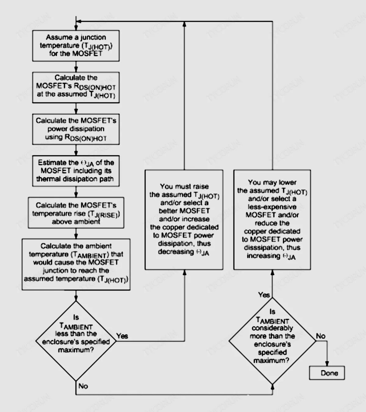
The figure above shows the iterative process of selecting each MOSFET (synchronous rectifier and switching MOSFET). In this process, the junction temperature of each MOSFET is an assumed value, and the MOSFET power consumption and allowable ambient temperature of the two MOSFETs are calculated.
This process ends when the limit of allowable ambient temperature reaches or is slightly higher than the maximum temperature we expect in the chassis (the power supply and the circuit it drives are installed in the chassis). The iterative process begins by assuming a junction temperature for each MOSFET.
Then, the individual MOSFET power consumption and allowed ambient temperature are calculated. This process ends when the allowable ambient air temperature reaches or slightly exceeds the expected maximum temperature of the chassis in which the power supply and the circuitry it drives are located.
Assuming a MOSFET junction temperature and then calculating the ambient temperature is a backwards approach. After all, the ambient temperature determines the MOSFET's junction temperature. However, it is easier to start the calculation from an assumed junction temperature than from the ambient temperature.
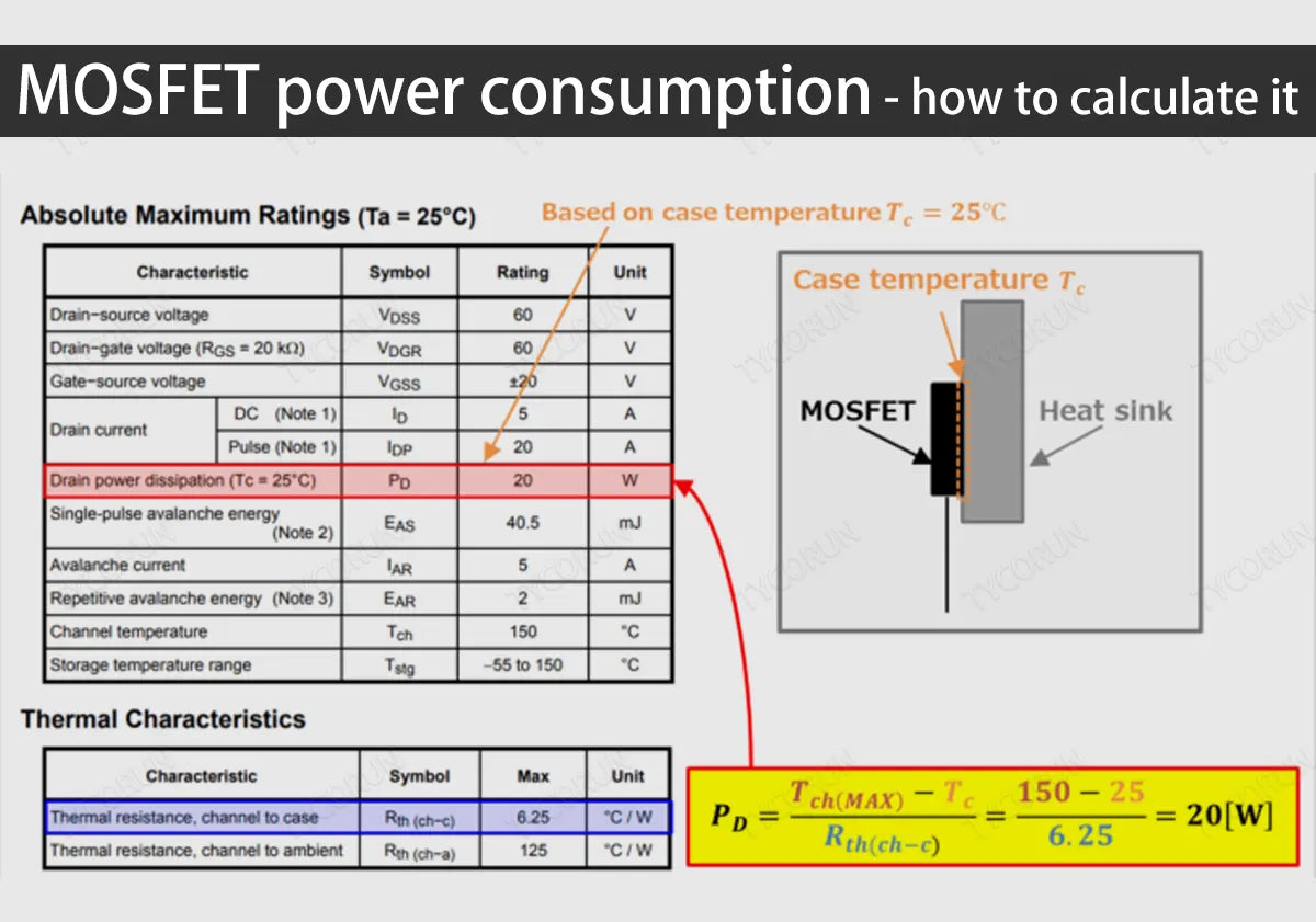
For switching MOSFETs and synchronous rectifiers, we can choose a maximum allowed junction temperature (TJ(HOT)) as the starting point for the iterative process. Most MOSFET data sheets only specify the maximum RDS(ON) at +25℃. The RDS(ON) of a MOSFET increases with temperature, with a typical temperature coefficient between 0.35%/℃ and 0.5%/℃.
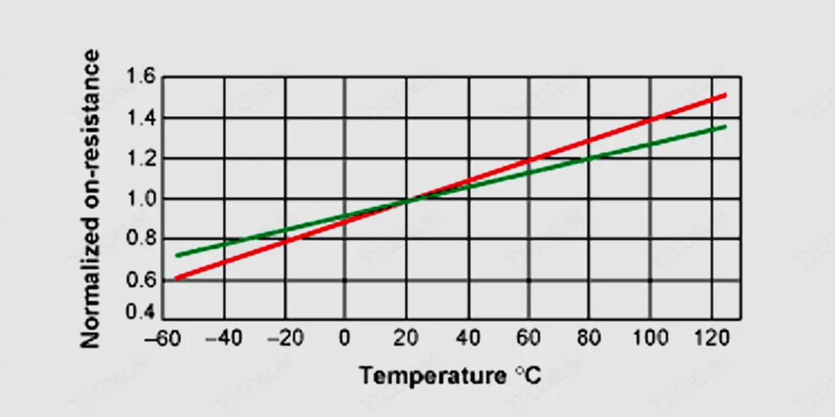
The temperature coefficient of the on-resistance of a typical power MOSFET is between 0.35% per degree (green line) and 0.5% per degree (red line). If unsure, use a worse temperature coefficient and the +25℃ specification of the MOSFET ( or +125℃ specification, if available) to approximate maximum RDS(ON) at selected TJ(HOT):
RDS(ON)HOT=RDS(ON)SPEC[1+0.005×(TJ(HOT)-TSPEC)]
Among them, RDS(ON)SPEC is the MOSFET on-resistance used in the calculation, and TSPEC is the temperature when RDS(ON)SPEC is specified. Using the calculated RDS(ON)HOT, the power consumption of the synchronous rectifier and switching MOSFET power consumption can be determined following the steps below:
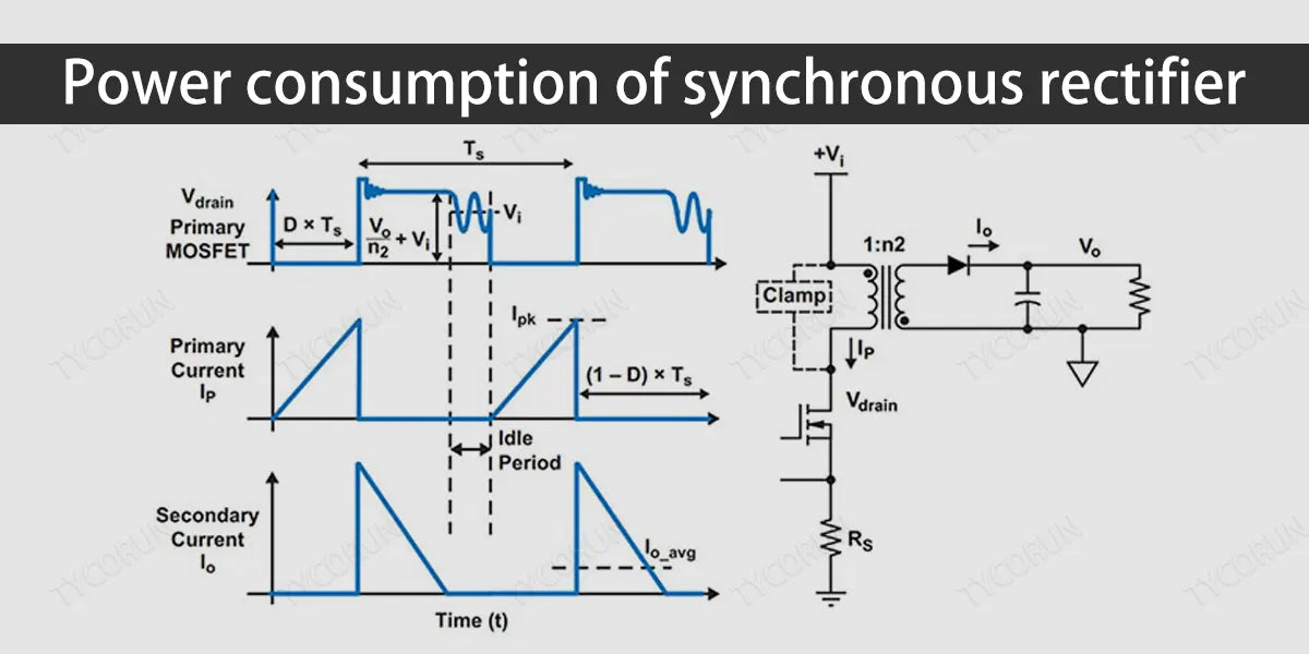
Power consumption of synchronous rectifier
Except for the lightest loads, under all other situations, the drain-to-source voltage of a synchronous rectifier MOSFET is clamped by the freewheeling diode during turn-on and turn-off. Therefore, a synchronous rectifier has almost no switching losses and its power consumption is easy to calculate.
Only resistive losses need to be considered. In the worst case, the losses occur when the synchronous rectifier is operated at its maximum duty cycle, that is, when the input voltage reaches its maximum.
Using the RDS(ON)HOT and operating duty cycle of the synchronous rectifier, we can approximately calculate its power consumption through Ohm's law:
PD synchronous rectifier=[ILOAD²×RDS(ON)HOT]×[1-(VOUT/VINMAX)]
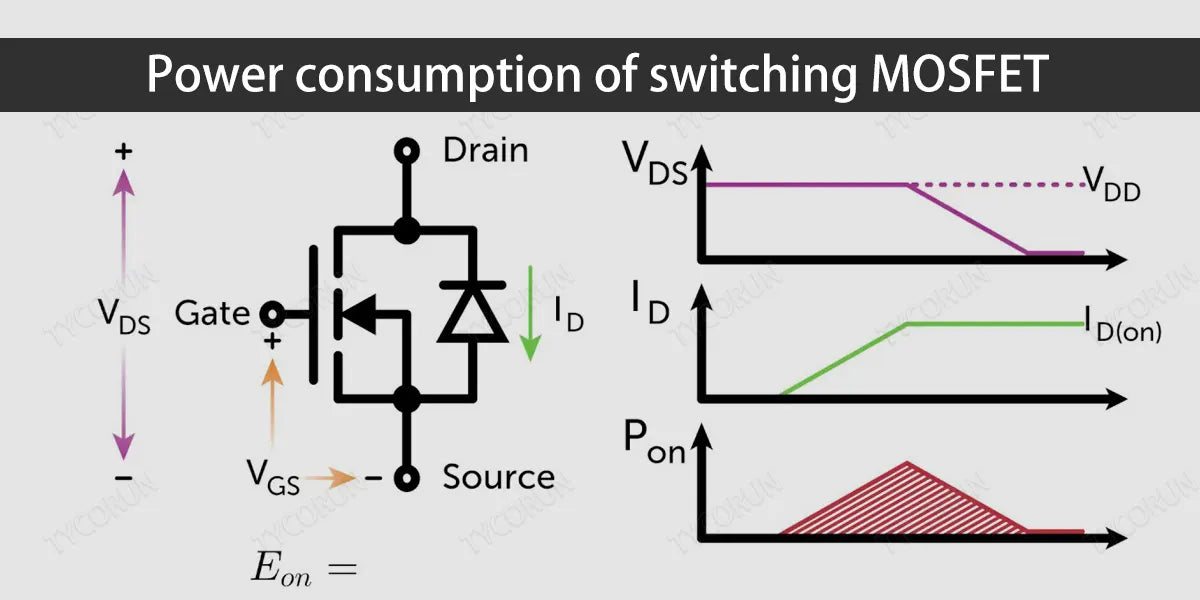
Power consumption of switching MOSFET
The resistive loss calculation of the switching MOSFET is very similar to that of the synchronous rectifier, also using its duty cycle (different from the former) and RDS(ON)HOT:
PD resistive=[ILOAD²×RDS(ON)HOT]×(VOUT/VIN)
The switching loss of a switching MOSFET is difficult to calculate because it depends on many factors that are difficult to quantify and often have no specifications, and these factors affect both the turn-on and turn-off processes. We can first evaluate a MOSFET using the following rough approximate formula, and then verify its performance through experiments:
PD switching=(CRSS×VIN²×fSW×ILOAD)/IGATE
Here, CRSS is the reverse transfer capacitance of the MOSFET (a parameter in the data sheet), fSW is the switching frequency, and IGATE is the absorption of the MOSFET gate driver when the MOSFET is in critical conduction (VGS is in the flat region of the gate charging curve) /source current.
Once the choice has been narrowed down to a specific generation of MOSFETs based on cost factors (the costs of different MOSFET generations vary widely), we can find a device within that generation that minimizes MOSFET power consumption.
This device should have balanced resistive and switching losses. Using a smaller (faster) MOSFET will increase the resistive losses more than it reduces in switching losses, while a larger (lower RDS(ON)) device will increase the switching losses more than it reduces in resistive losses.
If VIN changes, the switching MOSFET power consumption needs to be calculated separately under VIN(MAX) and VIN(MIN). The worst case scenario for MOSFET power consumption may occur at the lowest or highest input voltage. This MOSFET power consumption is the sum of two factors: resistive dissipation, which is highest at VIN(MIN) (higher duty cycle), and switching losses, which are highest at VIN(MAX) (due to the VIN² term).
A good choice should have approximately the same dissipation at both extremes of VIN, and maintain balanced resistive and switching losses over the entire VIN range. If the losses are significantly higher at VIN(MIN), resistive losses dominate. In this case, you can consider using a larger switching MOSFET (or connecting more than one tube in parallel) to reduce RDS(ON).
But if the losses are significantly higher at VIN(MAX), you should consider reducing the size of the switching MOSFET (or removing one MOSFET if multiple tubes are connected in parallel) to make it switch faster. If the resistive and switching losses have reached equilibrium, but the total MOSFET power consumption is still too high, there are several solutions:
- Change the definition of the problem. For example, redefine the input voltage range.
- Change the switching frequency to reduce switching losses, possibly using larger switching MOSFETs with lower RDS(ON).
- Increasing the gate drive current may reduce switching losses. The MOSFET's own internal gate resistance ultimately limits the gate drive current, effectively limiting the effectiveness of this approach.
- Adopt an improved technology MOSFET to achieve faster switching speed, lower RDS(ON) and lower gate resistance at the same time.
It is not possible to make finer adjustments to the size of the MOSFET outside a given condition because the range of device choices is limited. The bottom line in selection is that the MOSFET power consumption in the worst case must be able to be dissipated.
Power consumption of thermal resistance
The next step is to calculate the ambient temperature around each MOSFET at which the MOSFET junction temperature will reach the assumed value (follow the iterative process shown in figure above to determine the appropriate MOSFET to serve as the synchronous rectifier and switching MOSFET).
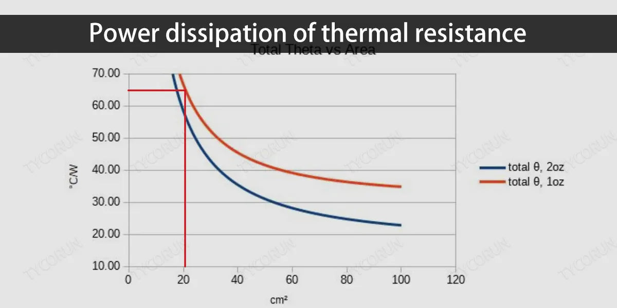
To do this, first determine the thermal resistance (ΘJA) of each MOSFET junction to ambient. It is relatively easy to measure ΘJA for a single device on a simple PCB, but it is difficult to predict the thermal performance of an actual power supply in a system where there are many heat sources such as LFP battery, competing for limited heat dissipation channels.
If multiple MOSFETs are used in parallel, the overall thermal resistance is calculated in the same way as the equivalent resistance of two or more parallel resistors. We can start with the MOSFET's ΘJA specification. For a single-tube core, 8-pin packaged MOSFET, ΘJA is typically close to 62℃/W.
Other types of packages, some with heat sinks or exposed heat conductors, generally have thermal resistances between 40℃/W and 50℃/W. The thermal resistance of different devices of the same package type, as well as similar packages from different manufacturers, varies and is related to the mechanical characteristics of the package, tube core size, and mounting and bonding methods.
The thermal information in the MOSFET data sheet needs to be carefully considered. The following formula can be used to calculate the temperature rise of the MOSFET tube core relative to the environment:
TJ(rise)=PD device total×ΘJA
Next, calculate the ambient temperature that will cause the tube core to reach the predetermined TJ(HOT):
T ambient=TJ(HOT)-TJ(RISE)
If the calculated T ambient is lower than the maximum rated ambient temperature of the chassis (meaning that the maximum rated ambient temperature of the chassis will cause the MOSFET's predetermined TJ(HOT) to be exceeded), one or more of the following measures must be taken: Increase the predetermined TJ(HOT), but do not exceed the maximum value specified in the data sheet.
- Choose a more appropriate MOSFET to reduce the MOSFET power consumption.
- Reduce ΘJA by increasing airflow or copper film around MOSFET.
- Recalculate T ambient (using a quick calculation table can simplify the calculation process, and only after many iterations can an acceptable design be selected).
On the other hand, if the calculated T ambient temperature is much higher than the maximum rated ambient temperature of the case, any or all of the following optional steps can be taken:
- Reduce the pre-ordered TJ(HOT).
- Reduce the copper covering area dedicated to MOSFET heat dissipation.
- Use cheaper MOSFETs.
These steps are just optional because in this case the MOSFET will not be damaged by overheating. However, through these steps, as long as the T ambient is higher than the maximum temperature margin of the case, we can reduce the board area and cost.
ΘJA specification
The largest source of error in the above calculation process comes from ΘJA. You should carefully read all notes in the data sheet regarding ΘJA specifications. General specifications assume the device is mounted on 1in² of 2oz copper film. The copper film dissipates most of the power, and the ΘJA varies greatly with different amounts of copper film. For example, a D-Pak package ΘJA with 1in² copper film will reach 50℃/W.
But if only the copper film is laid under the pin, ΘJA will be twice as high. If multiple MOSFETs are used in parallel, ΘJA mainly depends on the copper film area on which they are installed. The equivalent ΘJA of two devices can be half that of a single device, but must also double the copper film area.
In other words, adding a parallel MOSFET without adding copper film can halve RDS(ON) without changing ΘJA much. Finally, ΘJA specifications generally assume that no other devices are transferring heat to the thermal area of the copper film.
But at high currents, every component on the power path, even the PCB leads, generates heat. In order to avoid MOSFET overheating, the actual ΘJA needs to be carefully estimated and the following measures should be taken:
- Carefully study the available thermal performance information for the selected MOSFET.
- Check whether there is enough space to install more copper films, heat sinks and other devices.
- Determine if it is possible to increase airflow.
- Observe whether there are other devices that significantly dissipate heat on the assumed heat dissipation path.
- Estimate the excess heat or cooling from surrounding components or spaces.
Related posts: 12 volt 100ah deep cycle lithium battery, 12v 200ah deep cycle battery, battery stores near me