

With the development of large-capacity and modular energy storage converters work with off grid storage batteries, silicon carbide (SiC) devices have become a hit research topic due to their low-loss and high-temperature-resistant characteristics. However, the high switching speed of SiC devices makes them more sensitive to stray inductance in circuits, and the high-temperature operating environment also affects the long-term safe and reliable operation of the devices.
Therefore, the researchers focus on the low inductance design and heat dissipation design of SiC MOSFET-based power units for energy storage converters, as well as the overall design of the power units.
Main content:
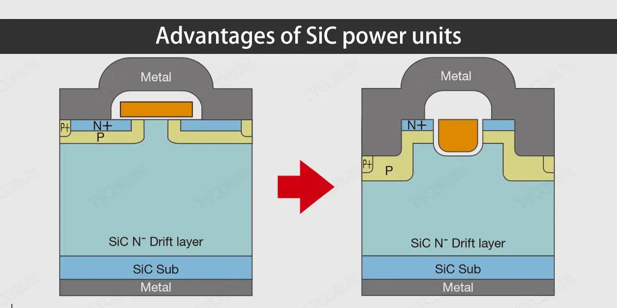
1. Advantages of SiC power units
The power of SiC power devices is very small, and the power unit composed of it is not suitable for use in high-power energy storage converters. As energy storage converter power units develop towards high integration, high operating frequency and large capacity, the research and design of energy storage converter power units composed of SiC devices are of great significance.
Since SiC power devices have high switching speeds, they will produce higher di/dt and du/dt than IGBTs, making them more prone to problems such as higher turn-off overvoltage, greater switching oscillation, and higher operating temperature. Therefore, the low-inductance design and heat dissipation design of the power unit are particularly important.
Although there are currently many literatures on stray inductance analysis of SiC power devices, there is a lack of low-inductance design of energy storage converter power units based on SiC MOSFETs.
For heat dissipation design, the module is generally attached to the radiator, and then the heat is dissipated through air cooling or water cooling. The literature proposes a new structure that directly connects the chip to Si-based microchannels through metal plating and thermal media materials, thereby eliminating the limitations of the module's multi-layer structure and improving the heat dissipation efficiency of the chip.
This article systematically analyzes the design method of energy storage converter power unit based on the new generation of power device SiC MOSFET.
2. Working principle of energy storage converter
The high-frequency isolated large-capacity energy storage converter adopts a modular cascade design, which can achieve higher voltage levels by connecting the same power units in series. The structure is more flexible and easy to expand the capacity. The capacity of a single converter can reach megawatts.
Using high-frequency low-loss power module SiC MOSFET, its maximum operating frequency can reach several hundred kHz, and can meet the overload requirements of 10% long-term overload operation and 20% overload operation for more than 1 minute, which can increase the switching frequency of the converter, thereby improving converter power density.
At the same time, from the perspective of high temperature resistance, compared with Si IGBT modules, it has higher thermal conductivity and heat flux density. The SiC MOSFET module itself has improved temperature tolerance, can withstand high temperature environments, and has good heat dissipation performance. The use of SiC MOSFET-based power modules is more conducive to the miniaturization, lightweight, and high-power density design of the converter, for example, DC to AC converter 500 watt.
Limited by the withstand voltage level of SiC MOSFET, a topology structure in which several power units are connected in series on the high-voltage side and in parallel on the low-voltage side is used to further expand the capacity and form a low-voltage, high-current DC port. When a large number of power modules are cascaded, uneven distribution of series voltages can easily cause overvoltage damage to devices, and unbalanced parallel currents can seriously restrict the capacity increase of the equipment.
In order to ensure voltage sharing between series power modules and current sharing between parallel power modules, corresponding control strategies are adopted.
On the series high-voltage side, the voltage balancing strategy of the power unit is divided into static voltage balancing and dynamic voltage balancing. Static voltage balancing relies on the energy consumption of the fan inside the unit, and dynamic voltage balancing is realized through software algorithm sequencing and modulation. The high-frequency transformer inside the high-voltage side power unit is vacuum epoxy cast to improve the insulation capability.
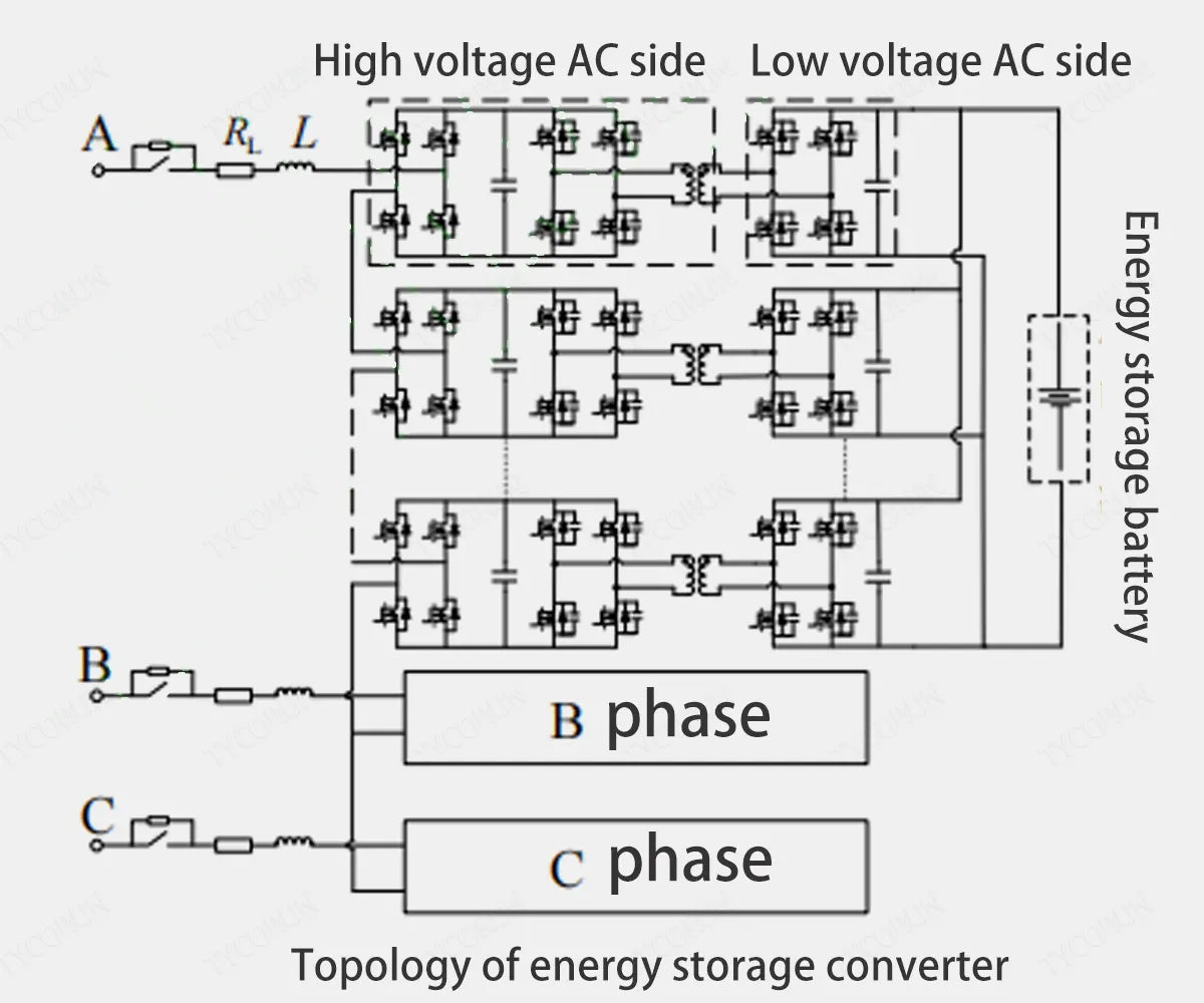
On the parallel low-voltage side, a power balance control method is used to achieve parallel current sharing. The high-voltage AC side power unit consists of a high-frequency transformer, two sets of H bridges and DC capacitors between them. The low-voltage DC side power unit consists of a set of H bridges and DC capacitors.
The H-bridge in the high-voltage AC module directly connected to the AC side is the AC/DC conversion unit. The H-bridge in the high-voltage AC module connected to the high-frequency transformer, the H-bridge of the low-voltage DC module and the high-frequency transformer form a dual active full-bridge DC /DC conversion.
Among them, the dual-active full-bridge DC/DC conversion topology can effectively suppress the double-frequency power fluctuations at all levels, obtain stable battery current, and extend LFP battery life. All power modules in the H-bridge are implemented by SiC MOSFETs.
3. How the power unit works
The SiC power unit includes a 10 kV high-voltage AC module and a 750 V low-voltage DC module. Both modules are based on an isolated H-bridge topology.
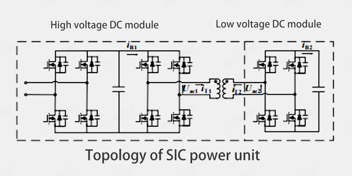
The dual-active full-bridge DC/DC conversion adopts a single phase-shift control method. The pulse signals of the two switching tubes corresponding to the diagonal corners of each full bridge are the same, and the pulse signals of the two switching tubes corresponding to each bridge arm are 180° apart.
When the home solar power system is running, by changing the phase shift angle between the two H bridges, the direction and magnitude of the transmission power can be adjusted to achieve two-way movement of energy. When the bridge arm voltage phase leads the AC grid voltage phase, energy flows from the DC side to the AC side, and the 12v battery is discharged; when the bridge arm voltage phase lags behind the AC grid voltage phase, energy flows from the AC side to the DC side and charge the battery.
The voltage waveform leakage inductance current under phase-shift control is shown in the figure below, where the phase-shift angle φ is the phase difference between the leading bridge HB1 and the lagging bridge HB2 during the power transmission process, and Ts is a switching cycle.
4. Low-inductance design of energy storage converter power unit
① Commutation circuit stray inductance
Let’s take the commutation process when the low-voltage side S22 and S23 are turned off as an example, to illustrate the phenomenon of power device turn-off voltage spikes. In loop A and loop B shown in the figure above, S22 and S23 are turning off. During the commutation process, the current iS passing through the power switch gradually decreases, while the current iD passing through the reverse diode is increasing. Rapid current changes act on the parasitic inductance flowing through the path and device, causing it to induce high-frequency voltage and form a commutation loop.
The voltage induced on the commutation circuit is superimposed on the DC bus voltage and acts together on the power devices S22 and S23, resulting in excessive du/dt, which forms a voltage turn-off peak. The peak voltage is expressed as:
In the formula: Umax is the shutdown overvoltage peak; L23 and L24 are the equivalent stray inductances of the power device and busbar respectively. This phenomenon occurs especially when the distributed inductance is large, the load current is large, and the power switch tube current decline time is short. Reducing the amount of parasitic inductance is an effective way to eliminate voltage turn-off spikes.
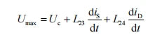
② Laminated busbar design
Depending on the structural layout of the power module, the laminated busbar has a variety of topologies. Considering the stray inductance balance problem of the commutation circuit, the laminated busbar used in this article has a symmetrical structure, which consists of two-level positive and negative copper conductors passing through the laminated structure, and insulating materials are superimposed between the conductors for hot pressing treatment.
The model is shown below.
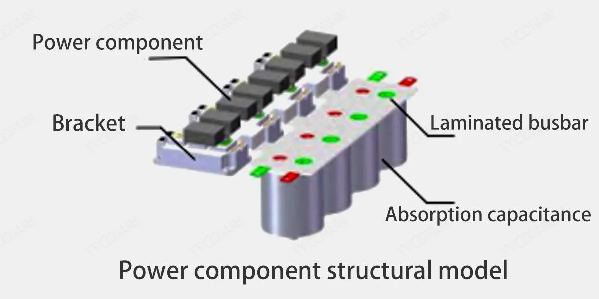
The parallel connection of multiple capacitors increases the stray inductance branches and improves the consistency, and the magnetic field is offset to reduce the loop inductance.
However, as the number of absorption capacitors increases, the amplitude of the inductor's effectiveness decreases. Therefore, after comprehensive consideration, four absorption capacitor structures are selected. The three-dimensional structural model of the laminated busbar with capacitor banks and power devices installed is as the figure below.
③ Radiator design
The size and layout of the radiator must match the laminated busbar and device placement, and is affected by factors such as radiator material, process, and fin parameters.
The radiator in this article is made of aluminum alloy, which has the characteristics of light weight and good heat dissipation. The rougher the surface of the material, the greater the surface emissivity and the worse the thermal conductivity, which is not conducive to heat dissipation. Therefore, smooth aluminum alloys are preferred.
Increasing the heat dissipation area is conducive to reducing thermal resistance, so increasing the number of fins can improve heat dissipation efficiency. On the other hand, too many fins will cause the size of the radiator to be larger, which is not conducive to the miniaturization and lightweight design of the power unit, and according to comprehensive consideration, the number of fins should be 15.
The total thermal resistance of the forced air-cooled radiator in the high-voltage AC module is Rth_h=0.7944 ℃/W, and the total thermal resistance of the radiator in the low-voltage module is Rth_l=0.7087 ℃/W. At full load, the loss of SiC MOSFET is about 150 W.
In the simulation software, the heat dissipation calculation is performed for a radiator and 4 SiC modules, and the maximum temperature rise value of the power device is required to be T≤40 K. In order to simplify the analysis, the thermal radiation heat dissipation is ignored, and the temperature rise change (T) curve of the power device under different inlet wind speeds (v) is obtained as shown in the figure below.
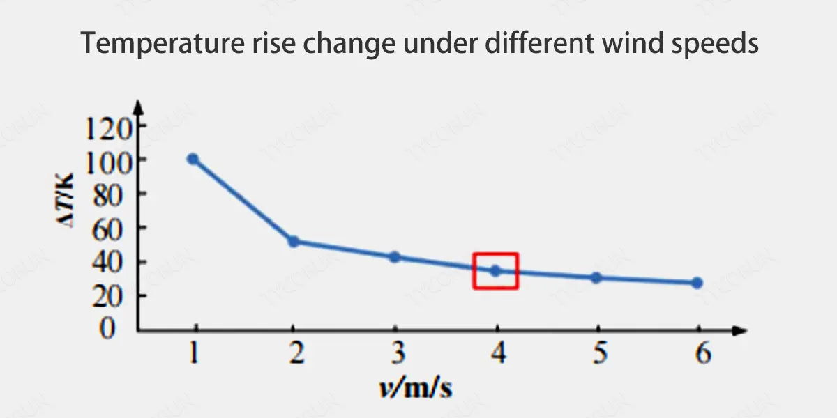
From the figure, we can see that when the wind speed is less than 2m/s, the maximum temperature rise of the power device decreases rapidly as the wind speed increases; when the wind speed is greater than 4 m/s, increasing the wind speed no longer has the obvious effect of reducing the temperature rise. When the wind speed is 4 m/s, the maximum temperature rise of the power device meets the heat dissipation needs, so it is recommended that the wind speed flowing into the radiator should be not less than 4 m/s.
5. Layout of SiC MOSFET energy storage converter power component
The design of the energy storage converter power unit based on SiC MOSFET is described below, and the corresponding component layout is shown in the figure below.
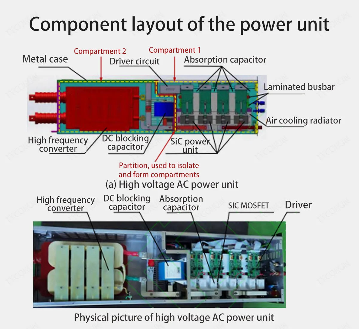
The power unit is composed of modular SiC power devices, high-frequency converters, absorption capacitors, DC blocking capacitors, laminated busbars, air-cooled radiators and metal casings.
The metal casing is designed with separate compartments. The compartments are connected to each other through the air duct of the air-cooled radiator for convection heat exchange.
In compartment 1, the SiC power device is placed on the surface of the air-cooled radiator, and the absorption capacitor is listed on the first side of the air-cooled radiator. On the side, it is connected to the SiC power device through the laminated busbar. The SiC power device drive circuit and control circuit are fixed on the metal casing, and the power is taken from the switching power supply connected to the absorption capacitor to achieve high-level energy taking.
In the compartment 2, the capacitor is connected between the module and the high-frequency transformer, and is fixed on the metal casing respectively. The output of the high-frequency transformer adopts a knife-shaped contact structure.
The AC side interface copper bar is placed in front of the power unit, passes through the Hall sensor and is fixed on the front side panel. The high frequency side interface is the secondary output of the high frequency transformer, that is, a knife-shaped contact with a wall bushing structure. The laminated busbar connects the positive and negative terminals of the snubber capacitor to the measurement terminals located on the front panel to facilitate measurement of the capacitor voltage.
This solution uses a laminated busbar structure, which can reduce loop inductance and reduce the overvoltage level during the switching process of the device. The module fan is automatically turned on when the absorbed capacitor voltage is higher than a certain value. While air cooling dissipates heat, it can also ensure voltage equalization among all modules in the power cabinet during the uncontrolled rectification charging stage.
Related posts: MOSFET diode, MOSFET power consumption, battery state of charge