

What is the working principle of solar battery? Solar energy is a kind of radiant energy, which must be converted into electrical energy by means of an energy converter. This energy converter that converts light energy into electrical energy is called a solar battery. How does solar battery convert light energy into electricity? The following is a brief introduction by taking a single crystal silicon solar battery as an example.
The working principle of solar battery is based on the photovoltaic effect of the semiconductor PN junction. The so-called photovoltaic effect, in short, is an effect in which electromotive force and current are generated when an object is illuminated, the state of charge distribution in the object changes. When sunlight or other light hits the PN junction of the semiconductor, a voltage appears on both sides of the PN junction, called the photogenerated voltage. This phenomenon is known as the photovoltaic effect. This effect short-circuits the PN junction, which generates current.
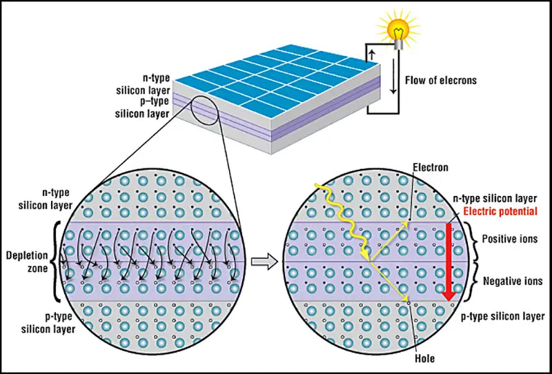
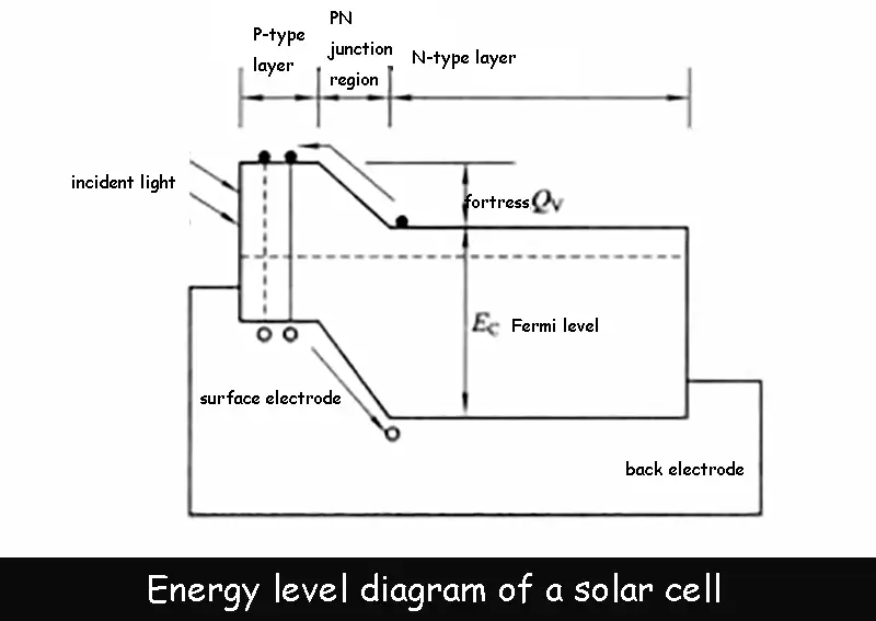
As we all know, atoms are made up of nuclei and electrons. The nucleus is positively charged and the electrons are negatively charged. Electrons revolve around atomic nuclei in certain orbits, just like planets revolve around the sun. The atoms of single crystal silicon are arranged according to certain rules, and there are 4 electrons in the outermost electron shell of the silicon atom. The outer electrons of each atom have fixed positions and are bound by the nucleus. Under the excitation of external energy, such as solar radiation, they will get rid of the shackles of the nucleus and become free electrons, and at the same time leave a vacancy in its original place, which is the so-called "hole" in semiconductor physics. Since electrons are negatively charged, holes appear to be positively charged. Electrons and holes are the electric charges that can move in single crystal silicon. In pure silicon, the numbers of free electrons and holes are equal. If impurity elements such as boron, aluminum, gallium or indium that can capture electrons are doped into the silicon crystal, a hole-type semiconductor is formed, which is referred to as a P-type semiconductor. If impurity elements such as phosphorus, arsenic or antimony that can release electrons are doped into the silicon crystal, an electronic semiconductor is formed, which is referred to as an N-type semiconductor. If these two semiconductors are combined, a PN junction will be formed at the interface due to the diffusion of electrons and holes, and a built-in electric field will be formed on both sides of the junction, also known as the barrier electric field. Since the resistance here is particularly high, it also becomes a barrier layer. When sunlight irradiates the PN junction, the atoms in the semiconductor release electrons due to the acquisition of light energy, and correspondingly generate electron-hole pairs, and under the action of the barrier electric field, the electrons are driven to the N-type region, Holes are driven to the P-type region, resulting in excess electrons in the N-type region and excess holes in the P-type region. As a result, a photo-generated electric field opposite to the direction of the barrier electric field is formed near the PN junction, as shown in Figure 8-7. Part of the photoelectric electric field cancels the potential barrier electric field, and the rest makes the P-type region positively charged, and the N-type region negatively charged, so that an electromotive force is generated in the thin layer between the N-type region and the P-type region, that is, photovoltaics. Electromotive force, when the external circuit is turned on, there is electric energy output. This is the basic principle of PN junction contact type single crystal silicon solar battery to generate electricity. If dozens or hundreds of solar battery is connected in series or in parallel to form a solar battery module, under the irradiation of sunlight, a considerable output power can be obtained.
In order to facilitate the reader to deepen the understanding of the introduction of the working principle of the solar battery, here is a brief introduction to the terms of several semiconductor physics involved.
1. Energy Band
Energy band is an important physical concept used to describe the state of electrons in crystals in solid quantum theory. In an isolated atom, electrons can only move in some specific orbits, and electrons in different orbits have different energies. Electrons can only take on some specific energy values, where each energy value is called an energy level. The product is composed of a large number of regularly arranged atoms, in which the energy level of the same energy of each atom becomes a slightly different energy level in the crystal due to the interaction, which looks like a band, so it is called energy. bring. The outer electrons of an atom are in higher energy bands in the crystal, and the inner electrons are in lower energy bands. The electrons in the energy band no longer move in closed orbits around their respective nuclei, but are shared by all atoms and move in the entire body.
2. Carriers
Carriers are particles that carry electric current. Whether it is a conductor or a semiconductor, the conduction effect is achieved by the directional motion of charged particles under the action of an electric field. Such charged particles are called carriers. Carriers in conductors are free electrons. There are two types of carriers in semiconductors, negatively charged electrons and positively charged holes. If the number of electrons in the semiconductor is much larger than the number of holes, and it is the electrons that play an important role in conduction, the electrons are called majority carriers, and the holes are called minority carriers. Conversely, holes are called majority carriers and electrons are called minority carriers.

3. Hole
Holes are a type of carrier in semiconductors. It has the same charge as the electron, but the opposite polarity. The energy band in the crystal that is completely occupied by electrons is called the full band or valence band, and the energy band that is not occupied by electrons is called the empty band or conduction band. The gap between the conduction band and the valence band is called the energy gap or forbidden band. If the electron jumps from the valence band with a lower energy level to the conduction band with a higher energy level due to external effects, there will be a very interesting effect: after the electron leaves, it will leave a vacancy in the valence band, According to the principle of electrical neutrality, the vacancy should be positively charged, and its charge is equal to that of the electrons. When the electrons near the vacancy move to fill the vacancy, it is equivalent to the vacancy moving in the opposite direction. Its function is similar to the motion of positively charged particles, and it is usually called positive hole, or hole for short. Therefore, under the action of the external electric field, the conduction in the semiconductor is not only produced by the movement of electrons, but also includes the contribution made by the movement of holes.
4. Donor
Any impurity doped into a pure semiconductor whose function is to provide conductive electrons is called a donor impurity, abbreviated as a donor. For silicon, if doped with elements such as phosphorus, arsenic, and antimony, their role is that of a donor.
5. Recipient
Any impurity doped into a pure semiconductor whose function is to accept electrons or provide holes is called an acceptor impurity, or acceptor for short. For silicon, such as doping boron, gallium, aluminum and other elements, the role they play is the role of the acceptor.
6. PN junction
On a semiconductor wafer, through some processes, part of the wafer is P-type (hole conduction) and the other part is N-type (electron conduction), then the area near the interface between P-type and N-type is called PN junction . The PN junction has unidirectional conductivity and is the basic structure of crystal diodes and the core of many semiconductor devices. There are many types of PN junctions: according to materials, there are homojunction and heterojunction; according to impurities, there are sudden change junction and gradual change junction; according to process, there are growth junction, alloy junction, diffusion junction, epitaxial junction and injection junction, etc.
Read more: China's abundant solar energy resources