

main content:
The main circuit of the charger is mainly responsible for converting the AC power of the power grid into a suitable DC power output, thereby charging the battery pack. It is generally composed of a rectifier part, a power factor correction (PFC) part, and a DC/DC conversion part. At present, the rectifier part of most chargers adopts diode rectifier bridge, and the structure is relatively simple, so the following content will mainly analyze the circuit topology of the other two parts.
1. Power Factor Correction (PFC) circuit topology
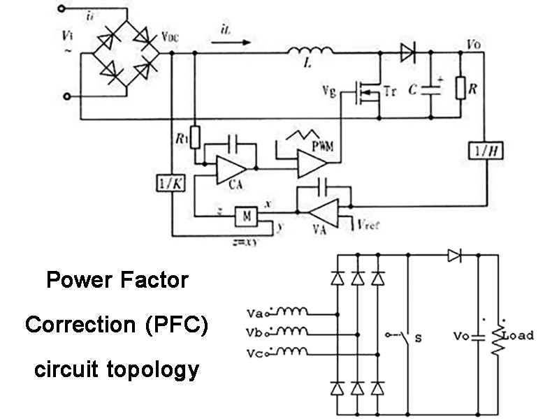
The main function of the power factor correction (power factor correction, PFC) circuit is to improve the power factor and suppress the high-order harmonics on the input grid side. PFC circuits can be divided into two categories: active power factor correction (APFC) circuits and passive power factor correction (PPFC) circuits according to whether active devices are used.
1) Passive power factor correction
In PPFC, the operating frequency is generally consistent with the input AC frequency, and the input current is subjected to a whole-wave phase shift. The PPFC circuit has a simple structure, and the power factor is not as high as that of the APFC. Usually, the power factor can be increased to 0.7~0.8. Moreover, due to the input of low-frequency current, the inductors and capacitors are large in size, which are easy to resonate with the grid impedance and cause damage to circuit components, which cannot be achieved. The dynamic compensation of reactive power and the suppression of harmonic current are not ideal, so this method is mainly used in power converters of medium and small power levels.
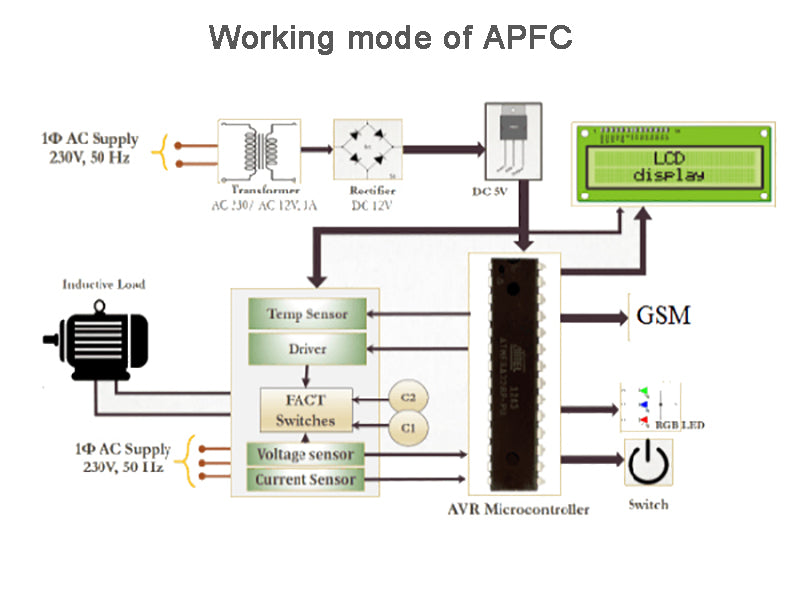
2) Active power factor correction
APFC works in high-frequency switching state. Compared with PPFC, it has the advantages of small size, light weight and high efficiency. The grid impedance and load impedance will not affect its compensation characteristics, and it can quickly and dynamically track and compensate for changing harmonics. The basic principle is to force the AC input current waveform to track the AC input voltage waveform through the control circuit, thereby improving the power factor, so it can be applied to a wider range of occasions and has a good development prospect.
There are four main circuit topologies of APFC: Buck, Boost, Flyback and Buck-Boost.
(1) Buck:
The input current is discontinuous, and the ripple is large, the filtering effect is poor, and the voltage stress on the switch tube is large, so it can only be used for step-down input.
(2) Boost:
The energy storage inductor at the input end makes the inductor current continuous, which can reduce the requirements for the input filter and suppress the transient high-frequency interference of the power grid to the main circuit. The peak value of the output voltage is higher than the peak value of the input voltage, and the current distortion rate is small. The control method is easy to implement, the capacitor energy storage increases, and the power-off protection lasts for a long time, so it has been widely used. Considering the power requirements of this design, this topology should be selected.
(3) Flyback:
Voltage-type control is adopted, the drive circuit is relatively simple, and the input and output are isolated by a transformer, but the magnetic core will generate unidirectional magnetization, which is difficult to achieve magnetic flux reset, and the utilization rate of the transformer is not high, so Commonly used in low-power (100W and below) and multi-output occasions.
(4) Buck-Boost:
The pulsation of the input and output voltage is large. In order to reduce the pulsation, a filter can be added on the input and output side. Because the voltage stress on the switch tube is very large, it is generally only used in the occasions of medium and small power output.
2. Working mode of APFC
Generally, by judging whether the inductor current is continuous, the APFC is divided into three operating modes: discontinuous mode (DCM), continuous mode (CCM), and critical mode (TM). In the range of small and medium power of several hundred watts, all three methods are used. Among them, the first two modes are more common, so these two modes are mainly described. In DCM mode, the input current distortion rate is small but the ripple is large, which requires high input filter circuit. The switch tube is easy to realize ZCS (zero current switching), and the diode does not need to bear the reverse recovery current. The peak current value is very large, the stress of the switch device increases, and its turn-on loss increases, so it is mostly used in low-power occasions, generally below 500W. In CCM mode, the input current ripple is small, the total harmonic distortion (THD) is small, the electromagnetic interference is small, and the requirement for the input filter is low, which limits the effective value of the current and reduces the conduction loss of the device, which is more suitable for high power Occasionally, Figure 1 shows the corresponding waveforms in the CCM mode of the Boost circuit.
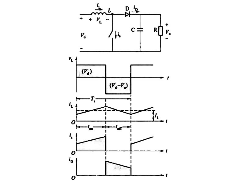
Figure 1 Corresponding waveforms in the CCM mode of the Boost circuit
3. Control strategy of APFC
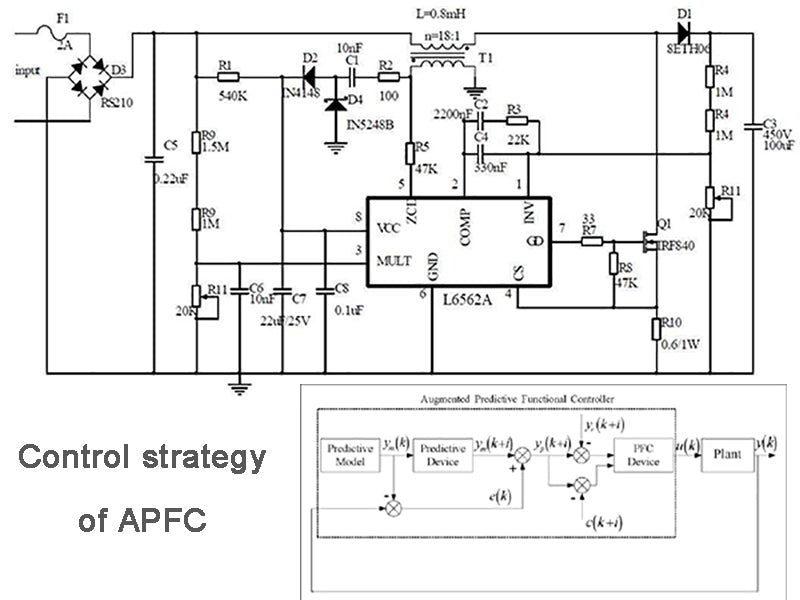
In terms of the selection of APFC control strategies, current control is currently the most used. This current control multiplies the output error signal of the voltage and the input signal through a multiplier, and then works with the collected current signal to control the on-off of the switch. The input current usually carries a little ripple of the switching frequency. Based on the basic structure of topology selection, the current amount of feedback can be divided into three common control methods: peak current control (PCMC), hysteresis current control (HCC), and average current control (ACMC). Figure 2 shows the three types. Comparison of control strategies.
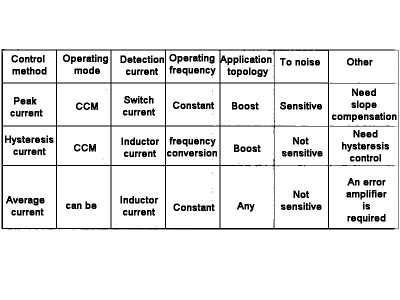
Figure 2 Comparison of three control strategies
1) Peak current control (PCMC) method
The advantages of peak current control are:
① The transient closed-loop response is relatively fast, and it can quickly respond to changes in input voltage and output load;
②The control loop design is easy;
③ With instantaneous peak current limiting function, etc.;
④It has a simple and automatic magnetic balance function.
When the power is constant, when the input voltage is low, the current peak value is large and easily affected by noise. It is necessary to add ramp compensation at the input end of the comparator to slow down the sub-harmonic oscillation when the duty cycle is greater than 0.5. In PFC circuits, PCMC is gradually no longer widely used.
2) Hysteresis current control (HCC) method
The Boost circuit uses HCC control, which is the simplest in comparison. In this control mode, the current dynamic response is fast, and the inductor current rises. When the upper limit of the predetermined hysteresis band is reached, the logic drive output changes from negative to positive, so that the switch tube is turned off, resulting in a decrease in the inductor current. As the current decreases to the lower limit of the hysteresis band, the switch is turned on again, and this cycle makes the inductor current track the change in the output value of the multiplier. The variable detected by hysteresis control is the inductor current. Compared with peak current control, there is no need to add a modulation signal. A logic link is added to the output of the comparator to generate a current hysteresis band, which can obtain a wide current bandwidth and hysteresis band. The bandwidth of the current ripple determines the size of the current ripple, which has a great impact on the switching frequency and system performance. The switching frequency is not constant, and it is easy to cause the dead zone of the current to zero and electromagnetic interference problems. Since the load greatly affects the switching frequency, it is difficult to minimize the design by setting the filter at the lowest frequency.
3) Average current control (ACMC) method
The ACMC control mode collects the inductor current, and a relatively smooth input current waveform can be obtained through control. The ACMC method has the following characteristics: the frequency of the switching tube is fixed, and it is not easily affected by noise; the THD is small, which reduces the error between the peak value and the average value of the inductor current; theoretically, it can detect the current on any topology branch; it is generally applicable to large, In medium power applications, it is most widely used in PFC circuits.
4.DC/DC conversion circuit topology
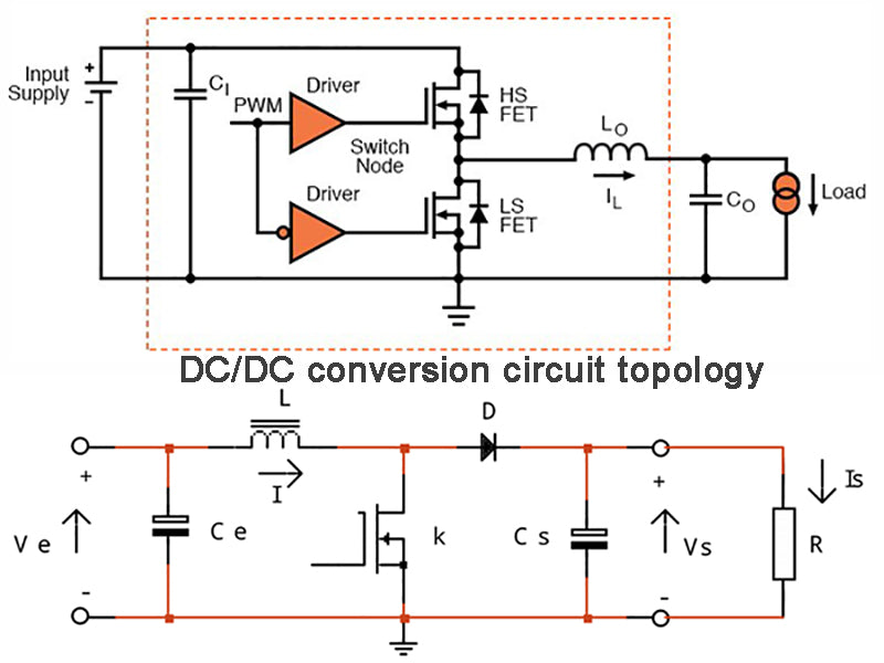
At present, most of the DC/DC conversion parts of the main circuit of the charger use full-bridge converters. On the one hand, it is due to the requirements of high-power applications. On the other hand, the utilization rate of full-bridge power converters is high, and the voltage and The current stress is small. The control methods of the full-bridge converter mainly include unipolar control, bipolar control and phase shift control. In recent years, phase-shift control has been widely used in full-bridge converters. It is mainly divided into two types: one is that the switches of the leading and lagging bridge arms are turned on at zero voltage, which is called phase-shift control ZVS-PWM full-bridge For the DC converter, the other is that the switch tube of the leading bridge arm is turned on for ZVS, and the switch tube of the lagging arm is turned off by ZCS, which is called phase-shift control ZVZCS-PWM full-bridge DC converter. The following will mainly introduce the topology of the ZVZCS-PWM converter.
1) Add saturation inductance and DC blocking capacitor to the primary side
The ZVZCS full-bridge converter with saturable inductance and DC blocking capacitor on the primary side adds saturable inductance on the primary side and the capacitor connected in parallel on the switch tube to perform LC resonance, so that the switch tube can realize ZVS turn-on, but the primary-side inductance loss is relatively large, and the frequency is relatively high. high, which is not conducive to the improvement of the overall efficiency. The DC blocking capacitor can reset the primary current during the commutation period, thereby realizing ZCS (ZCS zero current switching). During the power transmission period, the primary side provides energy for the DC blocking capacitor, and the stress of the switch tube increases.
2) The secondary uses an active clamp
The active clamp adopts hard switching. In one switching cycle, the clamp switch is turned on for a short time to charge the clamp capacitor. After the super front arm is disconnected, the clamp capacitor discharges to realize the primary current reset. The working time of the clamp switch is Very short, but still has some impact on the overall efficiency, and works with the clamping capacitor to slow down the loss of duty cycle.
3) The secondary uses a coupled inductor
A coupled inductor and a diode are added to the secondary side. During the current commutation, by providing a loop for the secondary side current, the potential of the coupled inductor is used as a reverse blocking voltage, which is converted to the primary side to reset the primary side current. The control is relatively simple, there is no active switch, there will be no hard switching loss, and the stress of the primary current will not increase, so it is widely used.
4) A simple auxiliary circuit is added to the secondary
This simple auxiliary circuit consists of a small capacitor and two diodes with small margin. The auxiliary circuit contains neither energy consumption components nor additional active switches, and the control is simple. The capacitor is connected in parallel with the super-forearm switch. It resonates with the equivalent leakage inductance of the primary side of the transformer, so that the super front arm switch tube can achieve zero voltage turn-on (ZVS), and its auxiliary circuit provides back pressure for the primary side voltage, so that the lagging arm of the power switch tube can achieve zero current shutdown (ZCS) , thus making the full-bridge converter more efficient and less expensive.