
The preparation methods of thin-film electrode materials can be divided into two main categories: one is physical methods, and the other is chemical methods. There are many studies on the preparation of films by physical methods, and the properties of the films obtained are also better, mainly including magnetron sputtering (magnetron sputtering, MS), pulsed laser deposition (PLD), electron beam evaporation (EBE); chemical methods include electrostatic spray deposition (ESD), chemical vapor deposition (CVD), spin-coating technique and electroplating (electrodeposition). The chemical method is cheaper than the physical method to prepare thin film materials, but the control parameters increase, and it is not easy to obtain a thin film that meets the metering ratio.
Physical film production

The substrate to be coated is placed in a vacuum chamber, and the evaporation material is vaporized (or sublimed) by heating and deposited on the surface of the substrate at a certain temperature, thereby obtaining a thin film. This method of film formation is called evaporation coating, or evaporation for short. Evaporation is carried out in a high vacuum environment, which can prevent contamination and oxidation of the film, and is convenient to obtain a clean, dense film that meets the predetermined requirements. Compared with other film forming methods, the evaporation coating method is simpler in process, easy to operate, and lower in cost, so it is one of the commonly used methods.
The equipment for evaporation coating is a vacuum coating machine, which is mainly composed of three parts: a vacuum system, an evaporation device and a film thickness monitoring device. The vacuum system is used to obtain the necessary vacuum and provide the necessary conditions for film formation; the evaporation device is used to heat the coating material to evaporate; the film thickness monitoring device is used to monitor the film thickness to achieve the necessary film thickness.
Evaporation coating can be divided into resistance evaporation method, electron beam evaporation method, laser evaporation method, etc. according to the different evaporation sources. Resistance thermal evaporation is an evaporation method that uses the heat generated by the current passing through a heating source to heat the evaporated material. The evaporation source of resistance heating is commonly used with high melting point metals (tungsten, molybdenum, button) and graphite. In the resistance thermal evaporation method, since the film material is in direct contact with the evaporation source, the evaporation source may become impurities mixed into the film material and then co-evaporate; in addition, some film materials react with the evaporation source material, and the evaporation of the film material is limited by the melting point of the evaporation source, and the service life is short.
The electron beam evaporation method is an evaporation method that uses electron beams to bombard a part of the film material for heating. Its characteristics are: the energy can be highly concentrated, so that the local surface of the film material can obtain a high temperature; it can accurately and conveniently control the evaporation temperature; and it has a larger temperature adjustment range. Therefore, it can be applied to both high and low melting point film materials.
The laser evaporation method uses a laser beam as a heat source to heat the film material, and the power density of the laser beam can reach 106W/cm2 or more by focusing. It quickly vaporizes the film material by non-contact heating, and then deposits it on the substrate to form a film. The main advantage of the laser evaporation method is: it can realize the evaporation and deposition of the compound, and does not produce the phenomenon of fractionation. It can evaporate any high melting point material, and can wash and avoid the contamination of the film material, and at the same time can avoid the film surface charging when the electron beam evaporates. In addition, in the case where the substrate is not heated, a well-crystallized film can be obtained.
Sputtering coating is the use of positive ions generated by gas discharge to bombard the target as the cathode at high speed under the action of an electric field, so that the atoms (or molecules) of the target can escape and deposit on the surface of the substrate to be plated to form the required thin film. Sputter coating has the following characteristics.
①Since positive ions with kinetic energy of several hundred to several thousand electron volts bombard the target, the kinetic energy of the material particles obtained by sputtering is about tens of electron volts, so they have a strong adhesion to the substrate.
② The area of the evaporation source is small, while the area of the target material is larger during sputtering. Moreover, the sputtered particles reach the substrate surface to form a film after continuously colliding with the charged gas atoms (or molecules). However, during evaporation, the air pressure is lower than 1.33mPa, and the evaporated particles basically travel from the evaporation source to the substrate in a straight line. The thickness distribution of the sputtered film is more uniform than that of the evaporated film.
③Suitable for film formation of high melting point metals, alloys and compound materials.
The sputtering method can be divided into different sputtering film forming methods such as cathode sputtering, high frequency sputtering, magnetron sputtering, plasma sputtering and so on.
Radio frequency sputtering (RF method for short) is to form a high-frequency discharge between the target and the substrate under the action of a high-frequency electric field, and the positive ions and electrons in the plasma alternately bombard the target to produce sputtering. The characteristics of the RF method are: high sputtering rate, for example, when sputtering SiO2, the deposition rate can reach 200nm/min; the film is dense, with few pinholes, and high purity; and the film has strong adhesion.
Magnetron sputtering (magnetron sputtering) is a high-speed sputtering film forming method that confines and prolongs the movement path of electrons with a magnetic field, changes the direction of movement of electrons, improves the ionization rate of the working gas, and effectively utilizes the energy of electrons. The principle of magnetron sputtering is: electrons collide with argon atoms in the process of accelerating and flying to the substrate under the action of an electric field, ionizing a large number of argon ions and electrons, and the electrons flying to the substrate. The argon ions accelerate the bombardment of the target under the action of the electric field, sputtering a large number of target atoms, and the neutral target atoms (or molecules) are deposited on the substrate to form a film. The secondary electrons are affected by the Loren magnetic force of the magnetic field during the process of accelerating and flying to the substrate, and are confined in the plasma region near the target surface, where the plasma density is very high. The secondary electrons move circularly around the target surface under the action of a magnetic field, and the electrons have a long moving path. During the movement, it continuously collides with argon atoms and ionizes a large number of argon ions to bombard the target. After multiple collisions, the energy of the electrons gradually decreases, getting rid of the restraint of the magnetic field lines, away from the target, and finally deposited on the substrate.
Pulsed laser deposition (PLD) uses the huge energy of laser to irradiate the target. The target is heated and melted and vaporized in a very short time until it becomes plasma. The plasma is transported from the target substrate and finally condenses and nucleates on the substrate to form a thin film.
The advantages of pulsed laser preparation of thin films are: the energy (laser) is placed outside the vacuum chamber, which is easy to adjust; the use range is wide, and almost any substance that can be condensed can be prepared into a target. At the same time, due to the characteristics of the pulsed laser, the growth rate of the film can be arbitrarily adjusted as required; the film composition is easy to be strictly consistent with the target composition; the quality of the film is high, and the mutual diffusion between the film bottom and the substrate is small; it can be deposited directly on the stainless steel substrate without high temperature annealing treatment after deposition. Pulsed laser preparation of thin films also has some shortcomings. For example, when the laser heats the target, the temperature rises extremely fast, the gas expands sharply, and small droplets fall on the film, causing defects in the film.
Chemical film production

Chemical vapor deposition (CVD) is a classic thin film deposition technology, which supplies one or several compounds and elemental gases containing the elements constituting the thin film to the substrate, and generates the required thin film by means of gas phase action or chemical reaction on the substrate. The CVD method can control the composition of the film through the gas composition, the film deposition speed is fast, the preparation cost is low, and the large-area film can be prepared. Compared with evaporation film formation and sputtering film formation, the CVD method has uniform film layer and good coverage, and can also deposit the entire substrate. CVD method is divided into ordinary CVD method, plasma enhanced chemical vapor deposition (PECVD) and photochemical vaporization deposition method.
Electrostatic spray deposition (ESD) is to apply a higher voltage on the surface containing the precursor solution to generate aerosol, and then deposit the aerosol on the substrate through electrostatic deposition to make a thin film. The deposition efficiency of ESD is much higher than that of traditional CVD, and it is mostly used in the preparation of electrode film materials for lithium-ion batteries.
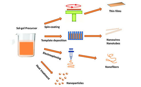
The sol-gel method (sol-gel) can be used not only to prepare ultra-fine powders, but also to thin film materials. The general process of the sol-gel method to prepare thin film materials is: the sol is prepared first, and then the method of coating or dipping is adopted to coat the sol on the substrate. After drying, heat treatment at a certain temperature to obtain a film on the substrate. The thickness of the coating film depends on the viscosity of the solution and the number of dips and brushes. The thin film prepared by the sol-gel method is typically a glass film. It is to immerse or brush or spray the alkoxide solution on the surface of the substrate, and then the coating film is digested in the air, agglomerated, dried, and finally sintered, and the formed film is uniformly cured on the surface of the substrate. The high-purity B2O3-SiO2 glass film prepared by this method can passivate alkali metal ions in electronic components such as integrated circuits. It has insulation, moisture resistance and oxidation resistance, and is a good electronic material.
Electroplating is a process of coating film by electrolysis. The research is "cathodic deposition", which is mainly used to prepare metal or alloy film materials. During electroplating, the substrate is immersed in the electroplating solution, which is used as the cathode, and the metal material to be plated (usually plate-shaped) is usually used as the anode and also immersed in the electrolyte. The electrolyte is a solution of a certain concentration of metal ions to be plated. Under electrification, the anode metal loses electrons and becomes metal ions and migrates into the electrolyte, while the metal ions in the solution migrate to the cathode. After obtaining electrons, they become metal atoms and deposit on the cathode to form a film. The basic requirements for the coating are: it has fine and compact crystals, the coating is flat, smooth and firm, without pinholes, etc. The quality of the coating is closely related to the surface condition of the substrate, the composition, concentration, pH, and current density and temperature of the electroplating solution. Generally, the surface of the substrate must be thoroughly cleaned and polished before plating, otherwise it is not easy to be plated or the plating layer is easy to blisters and fall off.